Electroluminescent display device

a display device and electroluminescent technology, applied in the direction of discharge tube luminescnet screens, discharge tube/lamp details, coatings, etc., can solve the problems of shrinkage problems, large display device size, and lack of hollow spacing, so as to improve the moisture blocking ability and enhance the reliability of the electroluminescent display device

Inactive Publication Date: 2013-05-23
WINTEK CHINA TECH LTD +1
View PDF2 Cites 29 Cited by
  • Summary
  • Abstract
  • Description
  • Claims
  • Application Information

AI Technical Summary

Benefits of technology

[0010]In the electroluminescent display device of the present invention, a single layer or a multi-layer ALD barrier is disposed in the inner surfaces of the substrates or at outer parts of the electroluminescent display device in order to improve the moisture blocking ability which may be influenced by the materials of the substrates and the sealant. The reliability of the electroluminescent display device may then be enhanced, and a touch positioning function may also be integrated into the electroluminescent display device.

Problems solved by technology

In the structure of the organic light emitting diode display device with glass fits, hollow spacing exists between two substrates and shrinking problem may occur when the size of the display device becomes larger.
Additionally, when the organic light emitting diode display device with glass fits and the touch panel are combined, touch operations may also damage the organic light emitting diode display device with glass frits.
Since the plastic substrate is not good at blocking moisture, moisture may penetrate the thin film transistor substrate 410 and the encapsulation substrate 420 made of plastic materials, and the display units 430 may then be damaged by the moisture.

Method used


Image

  • Electroluminescent display device
  • Electroluminescent display device
  • Electroluminescent display device

Examples


Embodiment Construction

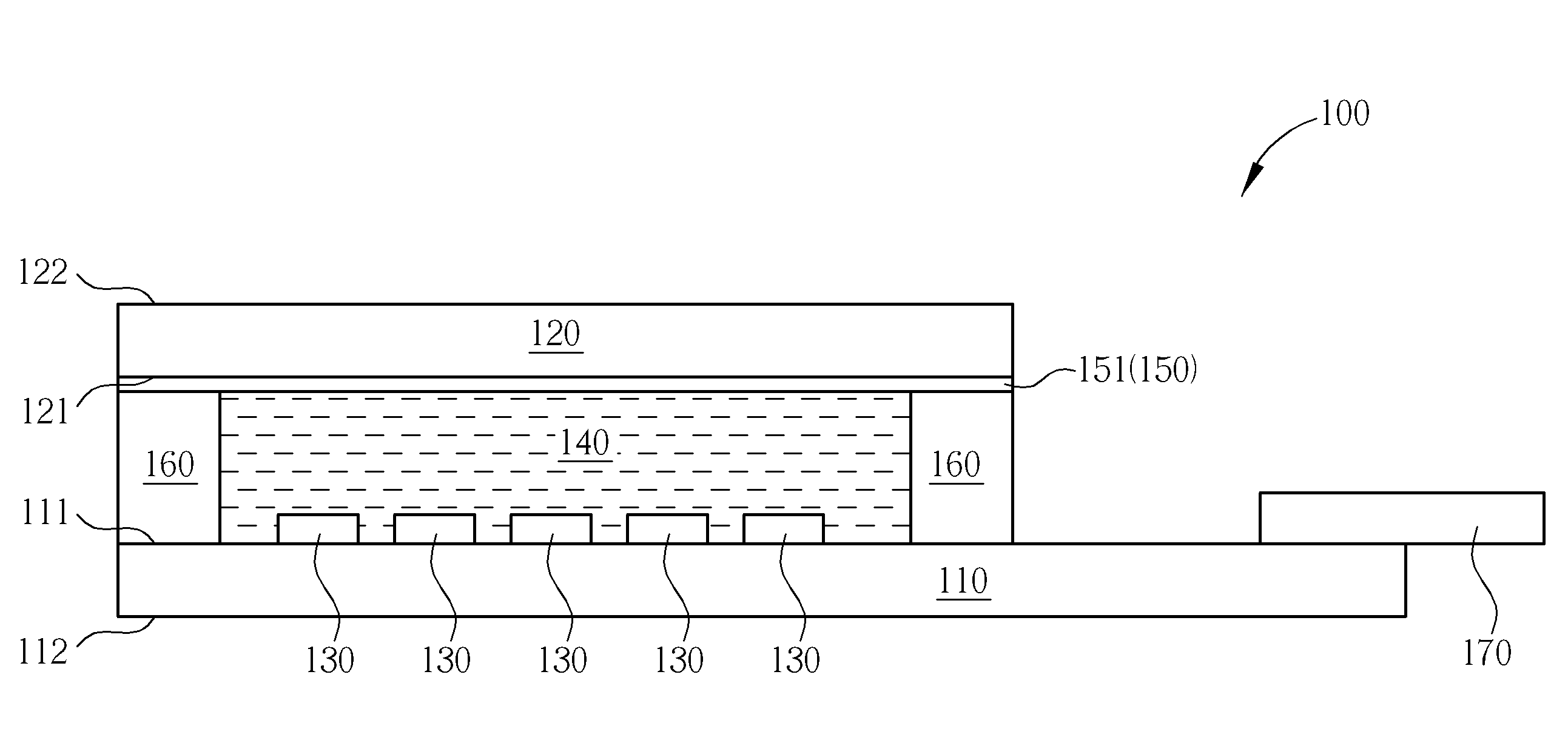
[0025]Please refer to FIG. 3. FIG. 3 is a schematic diagram illustrating an electroluminescent display device according to a first preferred embodiment of the present invention. Please note that the figures are only for illustration and the figures may not be to scale. The scale may be further modified according to different design considerations. As shown in FIG. 3, an electroluminescent display device 100 includes a main substrate 110, an encapsulation substrate 120, a plurality of display units 130, a sealant 140, and at least an atomic layer deposition (ALD) barrier 150. The main substrate 110 has a first inner surface 111 and a first outer surface 112. The encapsulation substrate 120 is disposed oppositely to the main substrate 110. The encapsulation substrate 120 has a second inner surface 121 and a second outer surface 122. The second inner surface 121 faces the first inner surface 111 and the second outer surface 122 faces a direction opposite to the first outer surface 112....


PUM

PropertyMeasurementUnit
thicknessaaaaaaaaaa
thicknessaaaaaaaaaa
sizeaaaaaaaaaa

Abstract

An electroluminescent display device includes a main substrate, an encapsulation substrate, a plurality of display units, a sealant, and at least an atomic layer deposition barrier. The main substrate has a first inner surface and a first outer surface. The encapsulation substrate is disposed oppositely to the main substrate. The encapsulation substrate has a second inner surface and a second outer surface. The display units are disposed on the first inner surface. The sealant is disposed between the main substrate and the encapsulation substrate, and the sealant covers the display units. The atomic layer deposition barrier covers at least one of the second inner surface and the second outer surface.

Description

BACKGROUND OF THE INVENTION[0001]1. Field of the Invention[0002]The present invention relates to an electroluminescent display device, and more particularly, to an electroluminescent display device with atomic layer deposition (ALD) barrier which is employed for improving the reliability and the life time of the electroluminescent display device.[0003]2. Description of the Prior Art[0004]Because of certain advantages, such as being color filter free, self-lighting, backlight module free, and having low power consumption, the electroluminescent display devices are regarded as a front runner to replace the conventional liquid crystal display device and become the mainstream display products of the next generation. Organic light emitting diode (OLED) display technology may be the most mature technology among all the electroluminescent display technologies.[0005]Glass frits are generally employed in the packaging process in the organic light emitting diode display technology. In the str...

Claims


Application Information

Patent Timeline
Patent Type & Authority Applications(United States)
IPC IPC(8): H05B33/04
CPCC23C16/45525H05B33/04H01L51/5253H01L51/524C23C16/40H10K50/841H10K50/844
Inventor CHANG, SHAO-JULIU, WEN-HONGHUNG, CHENG-CHIEHKANG, HEN-TAWANG, CHIH-YUAN
Owner WINTEK CHINA TECH LTD
Why Eureka
Try Eureka