

Scale of photoelectric encoder and manufacturing method of the same
- Summary
- Abstract
- Description
- Claims
- Application Information
AI Technical Summary
Benefits of technology
Problems solved by technology
Method used
Image

Examples
embodiment 1
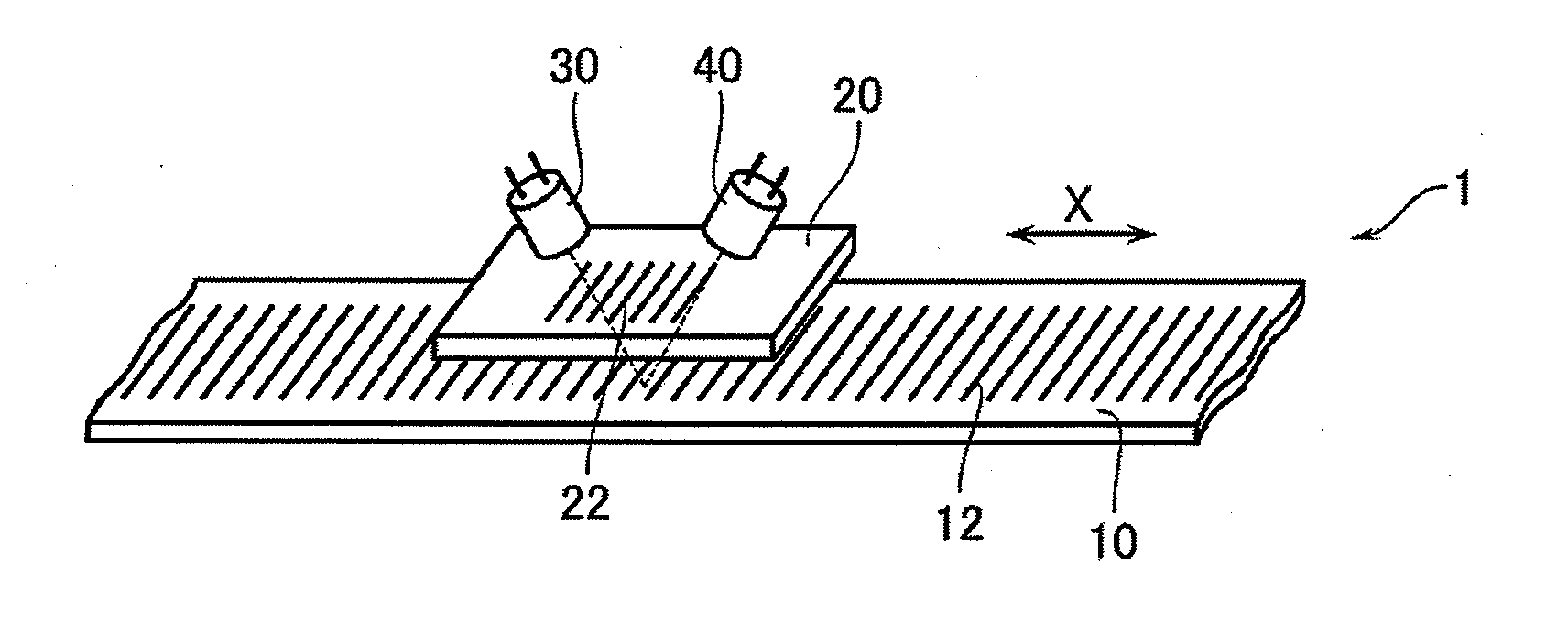
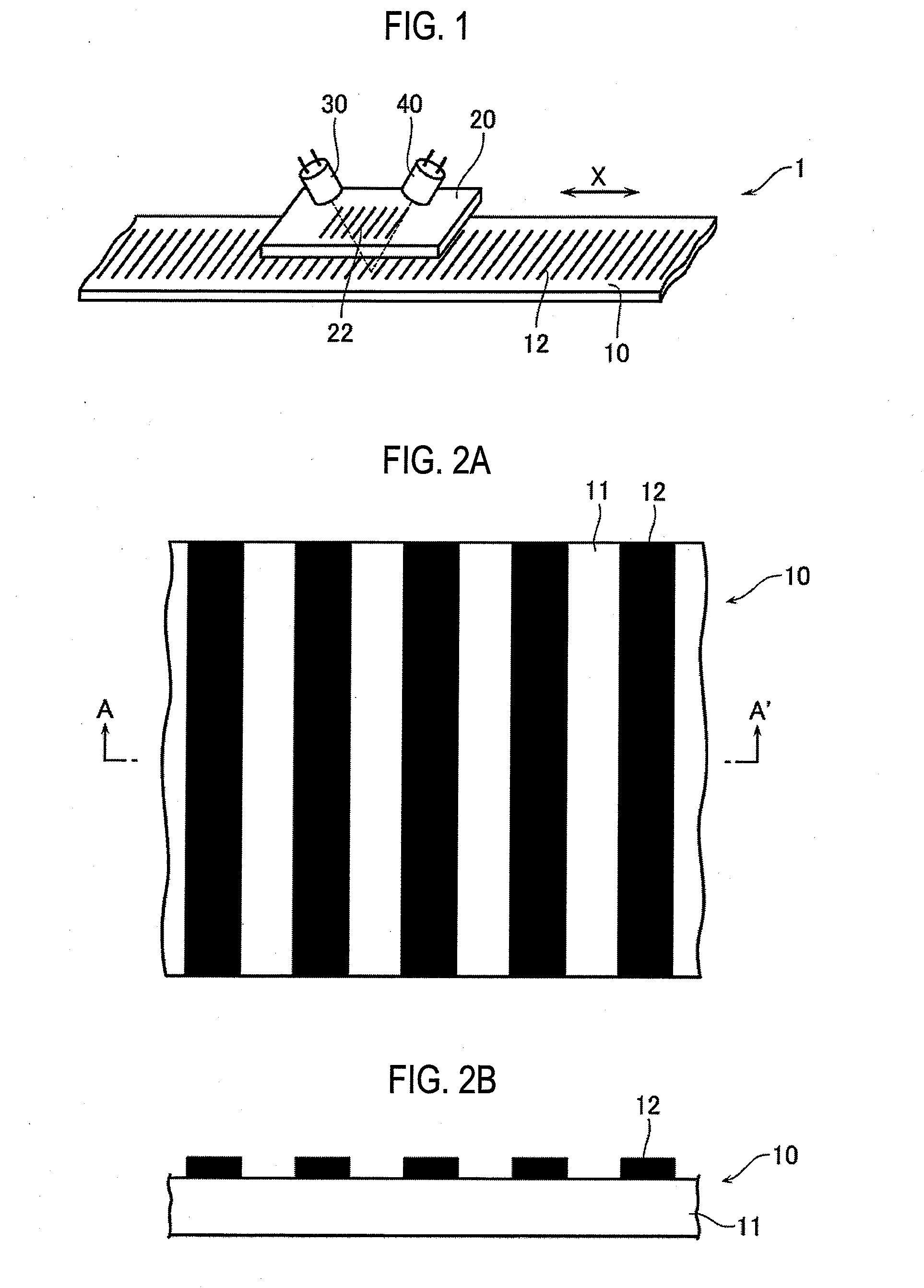
[0064]FIG. 1 is a perspective view which outlines the configuration of a photoelectric encoder 1 according to a first embodiment of the invention. The photoelectric encoder 1 has a main scale 10, an index scale 20, a light source 30, and a light receiver 40. The main scale 10 extends along a measurement axis X. The index scale 20 is moved relative to the main scale 10. The light source 30 applies light to the main scale 10 through the index scale 20. The light receiver 40 receives, through the index scale 20, light that is reflected from the main scale 10. The main scale 10 and the index scale 20 are formed with respective gratings 12 and 22 (graduations) at a prescribed pitch. As the main scale 10 and the index scale 20 are moved relative to each other, the phase relationship between the gratings 12 and 22 of the scales 10 and 20 varies. This variation is detected optically by the light receiver 40, whereby the position of the index scale 20 with respect to the main scale 10 is det...
embodiment 2
[0074]Next, a photoelectric encoder according to a second embodiment will be described with reference to FIG. 5. The second embodiment is different from the first embodiment in a main scale 10a (see FIG. 5). The items used in the second embodiment other than the main scale 10a are the same as used in the first embodiment, and hence will not be described in detail below.
[0075]A base member 11a of the main scale 10a is made of a metal, glass, ceramic, a carbon composite, or the like, and its top surface is roughened as shown in FIG. 5. The bottom surface of the base member 11a may also be roughened. As a further alternative, all the surfaces of the base member 11a may be roughened. Metal gratings 12a are formed as a light reflection film on the roughened top surface of the base member 11a. Since the underlying surface is roughened, the metal gratings 12a are formed by plating capable of leveling using a plating material that is, for example, nickel or chromium added with a brightener....
embodiment 3
[0080]Next, a photoelectric encoder according to a third embodiment will be described with reference to FIG. 8. The third embodiment is different from the first embodiment in a main scale 10b (see FIG. 8). The items used in the third embodiment other than the main scale 10b are the same as used in the first embodiment, and hence will not be described in detail below. In the main scale 10b, items having the same ones in the above embodiments will be given the same reference symbols as the latter and will not be described in detail.
[0081]Whereas the main scales 10 and 10a according to the first and second embodiments are reflection-type amplitude gratings, the main scale 10b according to the third embodiment is used as a reflection-type phase grating. In the main scale 10b, as shown in FIG. 8, a conductive film 13b is formed on the surface of a base member 11b by underlying surface treatment. The metal gratings 12a are formed on the top surface of the base member 11b through the condu...
PUM
 Abstract
Description
Claims
Application Information