Semiconductor device and manufacturing method thereof
a semiconductor and manufacturing method technology, applied in the direction of semiconductor devices, electrical devices, transistors, etc., can solve the problems of increasing the yield of a manufacturing process, and achieve the effects of high yield, high electrical characteristics, and high yield
- Summary
- Abstract
- Description
- Claims
- Application Information
AI Technical Summary
Benefits of technology
Problems solved by technology
Method used
Image

Examples
embodiment 1
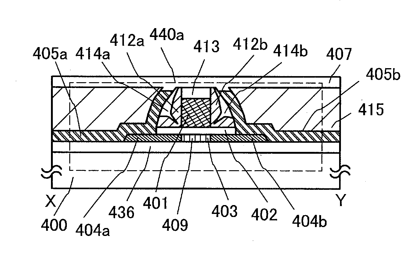
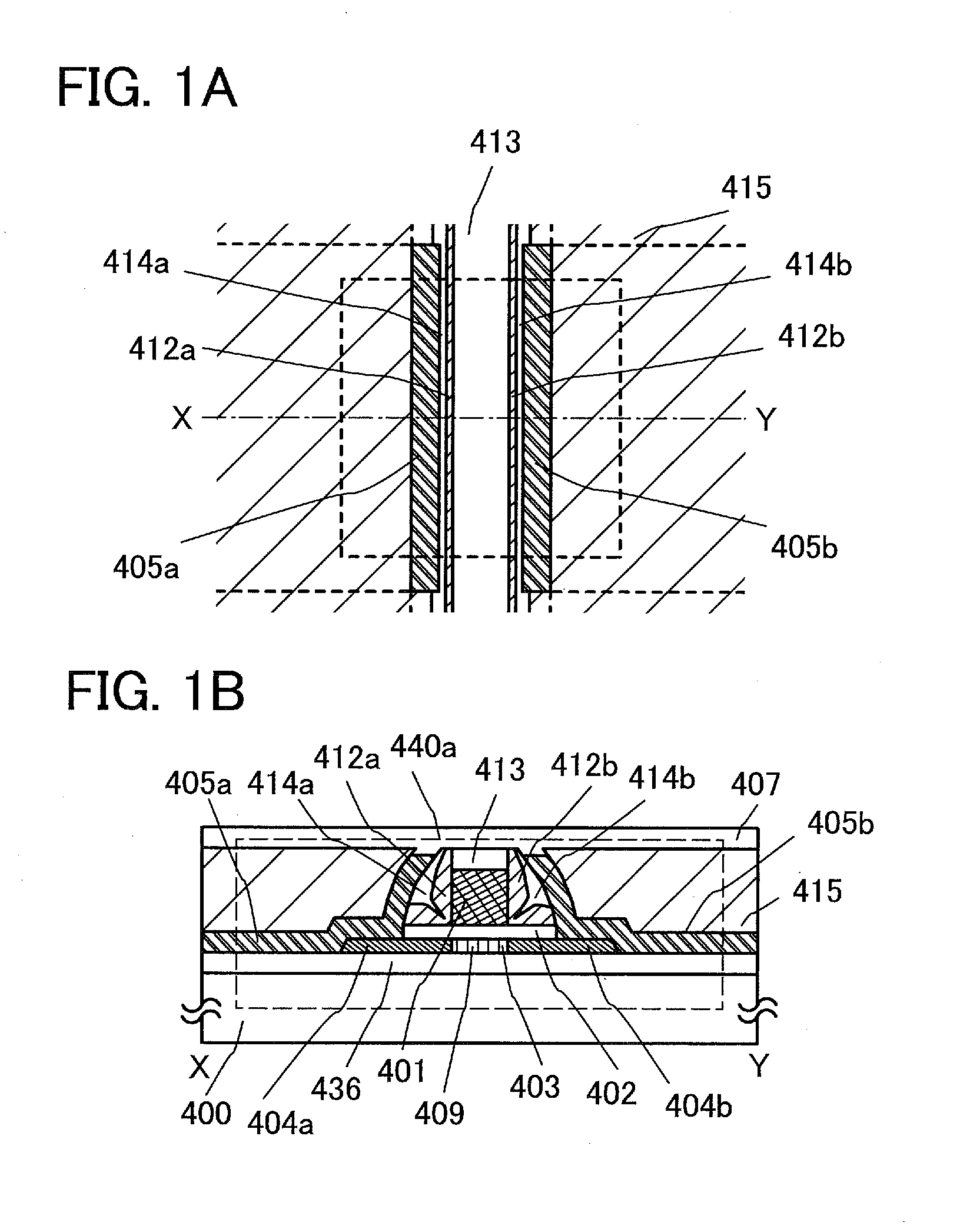
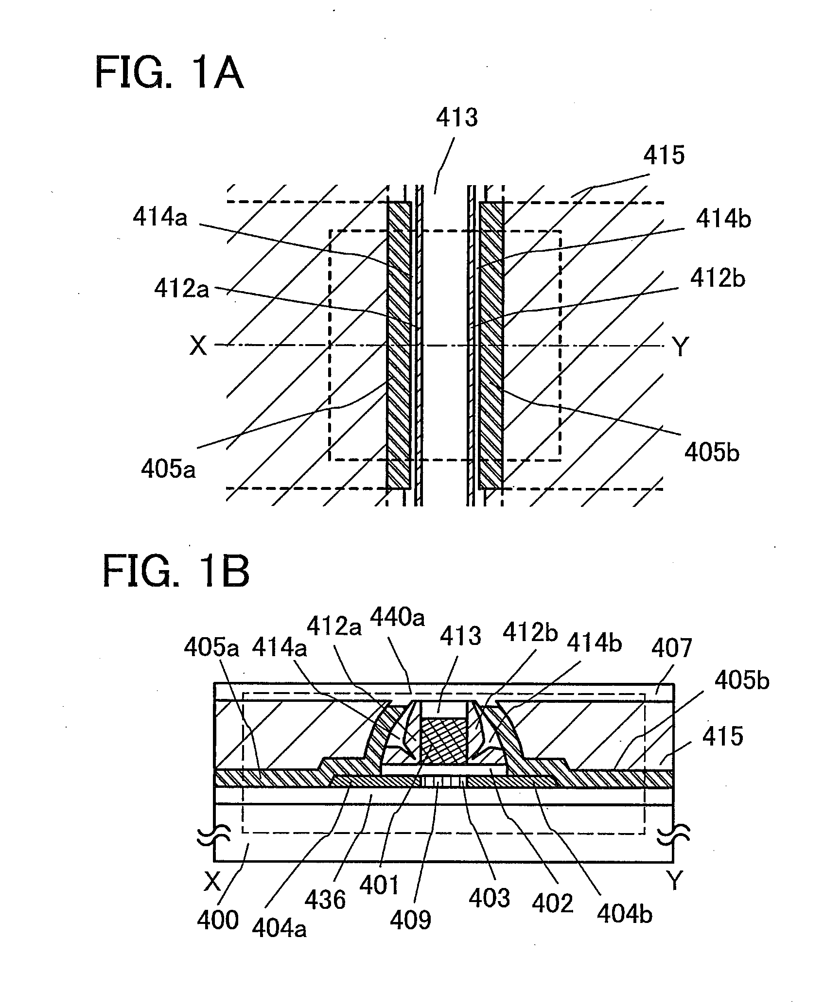
[0051]In this embodiment, an embodiment of a semiconductor device and a method for manufacturing the semiconductor device are described with reference to FIGS. 1A and 1B. In this embodiment, a transistor including an oxide semiconductor film is described as an example of the semiconductor device.
[0052]The transistor may have a single-gate structure in which one channel formation region is formed, a double-gate structure in which two channel formation regions are formed, or a triple-gate structure in which three channel formation regions are formed. Alternatively, the transistor may have a dual-gate structure including two gate electrode layers positioned above and below a channel formation region with a gate insulating film provided therebetween.
[0053]A transistor 440a illustrated in FIGS. 1A and 1B is an example of a top-gate transistor. FIG. 1A is a plan view and FIG. 1B is a cross-sectional view along dashed line X-Y in FIG. 1A.
[0054]As illustrated in FIG. 1B, which is a cross-se...
embodiment 2
[0203]In this embodiment, an example of a semiconductor device which includes the transistor described in this specification, which can hold stored data even when not powered, and which does not have a limitation on the number of write cycles, will be described with reference to drawings.
[0204]FIGS. 5A to 5C illustrate an example of a structure of a semiconductor device. FIG. 5A is a cross-sectional view of the semiconductor device, FIG. 5B is a plan view of the semiconductor device, and FIG. 5C is a circuit diagram of the semiconductor device. Here, FIG. 5A corresponds to a cross section along line C1-C2 and line D1-D2 in FIG. 5B.
[0205]The semiconductor device illustrated in FIGS. 5A to 5C includes a transistor 160 including a first semiconductor material in a lower portion, and a transistor 162 including a second semiconductor material in an upper portion. The transistor 162 is an example to which a structure of the transistor 440a described in Embodiment 1 is applied.
[0206]Here, ...
embodiment 3
[0243]In this embodiment, a semiconductor device which includes the transistor described in Embodiment 1 or 2, which can hold stored data even when not powered, and which does not have a limitation on the number of write cycles, and which has a structure different from the structure described in Embodiment 2 is described with reference to FIGS. 6A and 6B and FIGS. 7A and 7B.
[0244]FIG. 6A illustrates an example of a circuit configuration of a semiconductor device. FIG. 6B is a conceptual diagram illustrating an example of a semiconductor device. The semiconductor device illustrated in FIG. 6A will be described, and then, the semiconductor device illustrated in FIG. 6B will be described.
[0245]In the semiconductor device illustrated in FIG. 6A, a bit line BL is electrically connected to the source electrode or the drain electrode of the transistor 162, a word line WL is electrically connected to the gate electrode of the transistor 162, and the source electrode or the drain electrode o...
PUM
 Abstract
Description
Claims
Application Information
 - R&D Engineer
- R&D Manager
- IP Professional
- Industry Leading Data Capabilities
- Powerful AI technology
- Patent DNA Extraction
Browse by: Latest US Patents, China's latest patents, Technical Efficacy Thesaurus, Application Domain, Technology Topic.
© 2024 PatSnap. All rights reserved.Legal|Privacy policy|Modern Slavery Act Transparency Statement|Sitemap