

Inspection apparatus for semiconductor devices and chuck stage used for the inspectionapparatus
a technology of inspection apparatus and semiconductor devices, which is applied in the direction of individual semiconductor device testing, semiconductor/solid-state device testing/measurement, instruments, etc., can solve the problems of difficulty in obtaining transient characteristics necessary to conduct large current, failure of characteristics, and various processes carried out after, so as to reduce the inductance produced, the structure of the inspection apparatus becomes simple, and the electrical characteristics of semiconductor devices can be measured accurately.
- Summary
- Abstract
- Description
- Claims
- Application Information
AI Technical Summary
Benefits of technology
Problems solved by technology
Method used
Image

Examples
Embodiment Construction
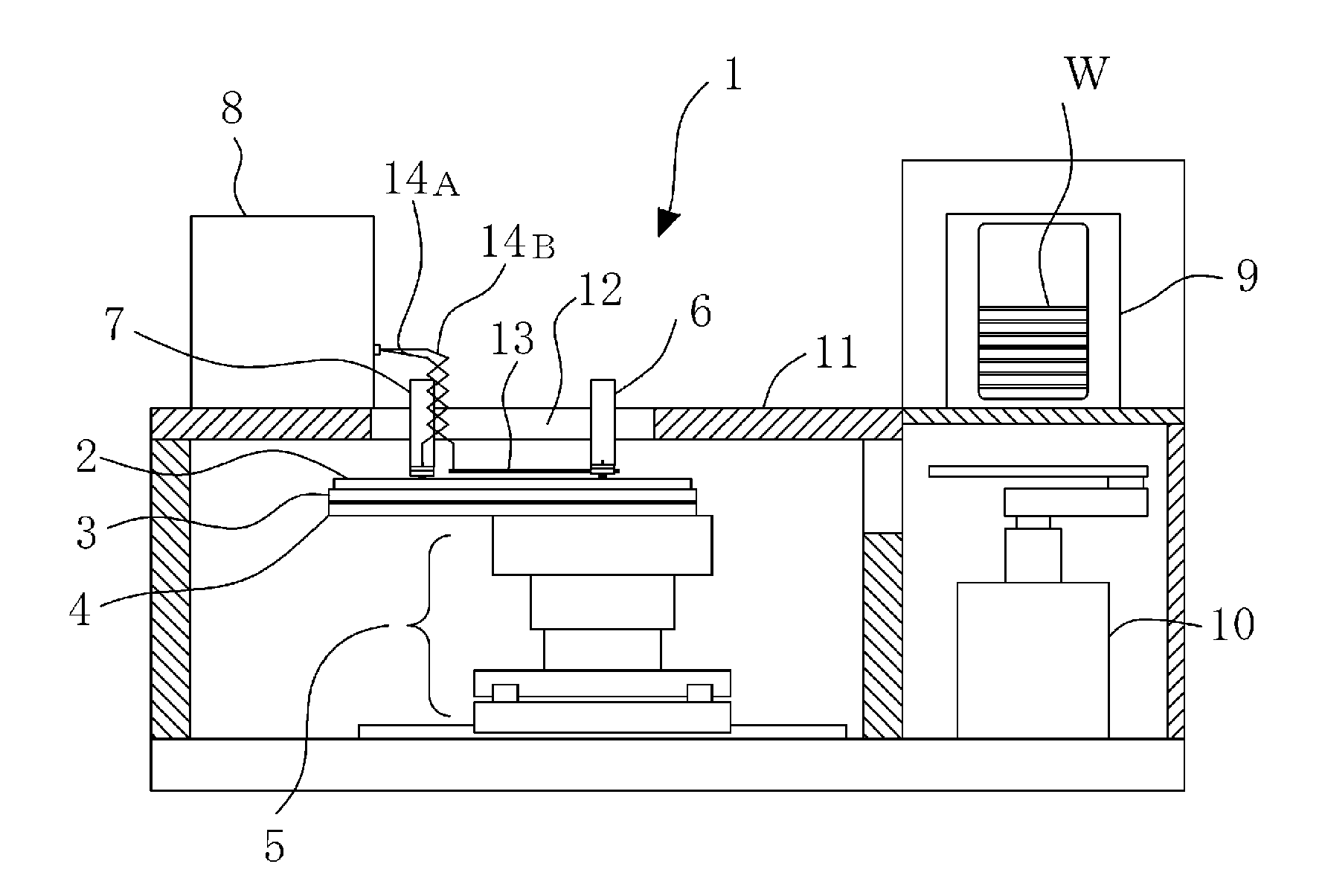
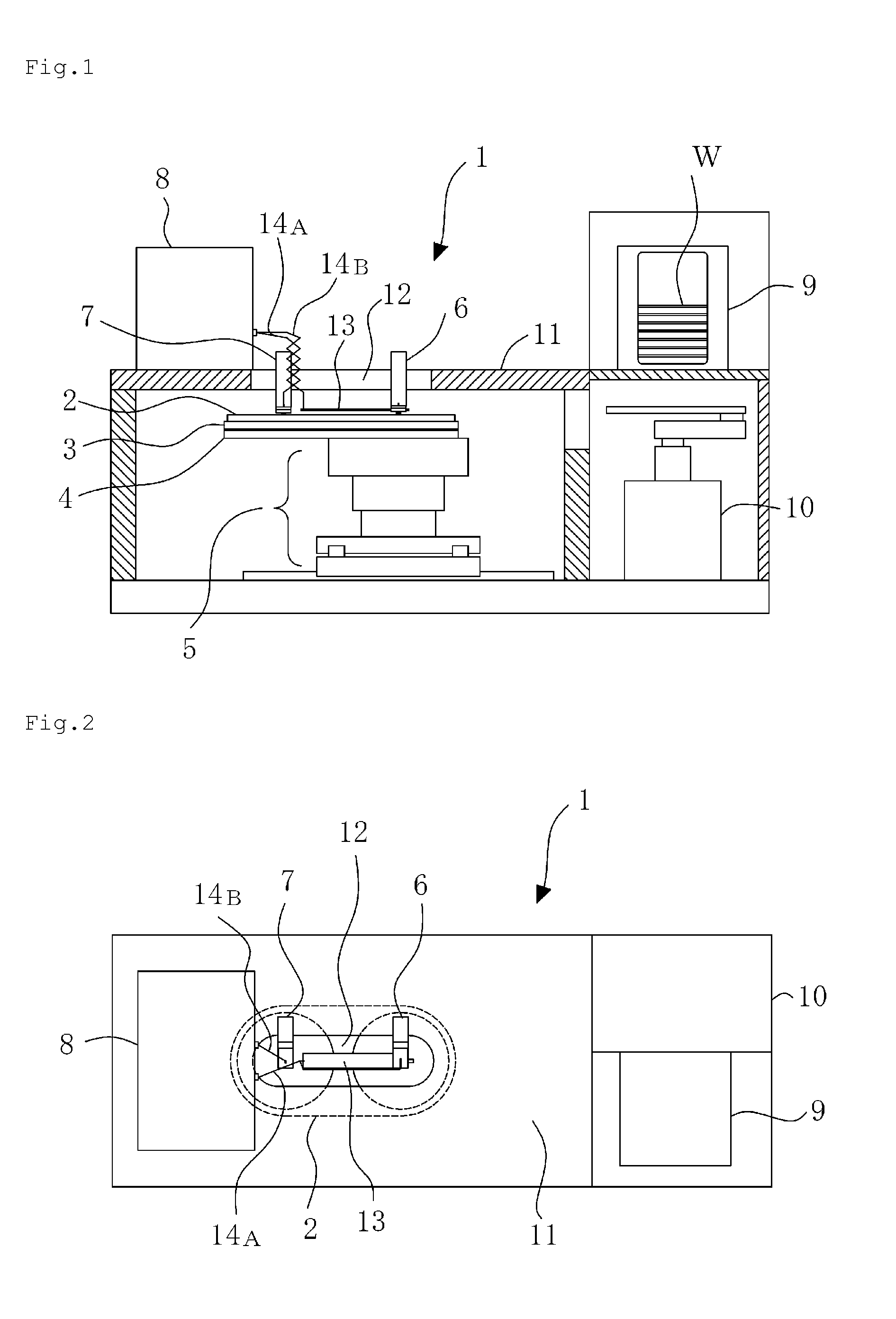
[0045]Hereinafter, the present invention is explained in detail with reference to the accompanying drawings picking up IGBT, which is one of power semiconductor devices, as an example of a semiconductor device inspected by the inspection apparatus of the present invention. As a matter of course, the power semiconductor devices inspected by the inspection apparatus of the present invention are not limited to IGBT, and the present invention is not limited to the illustrated examples.
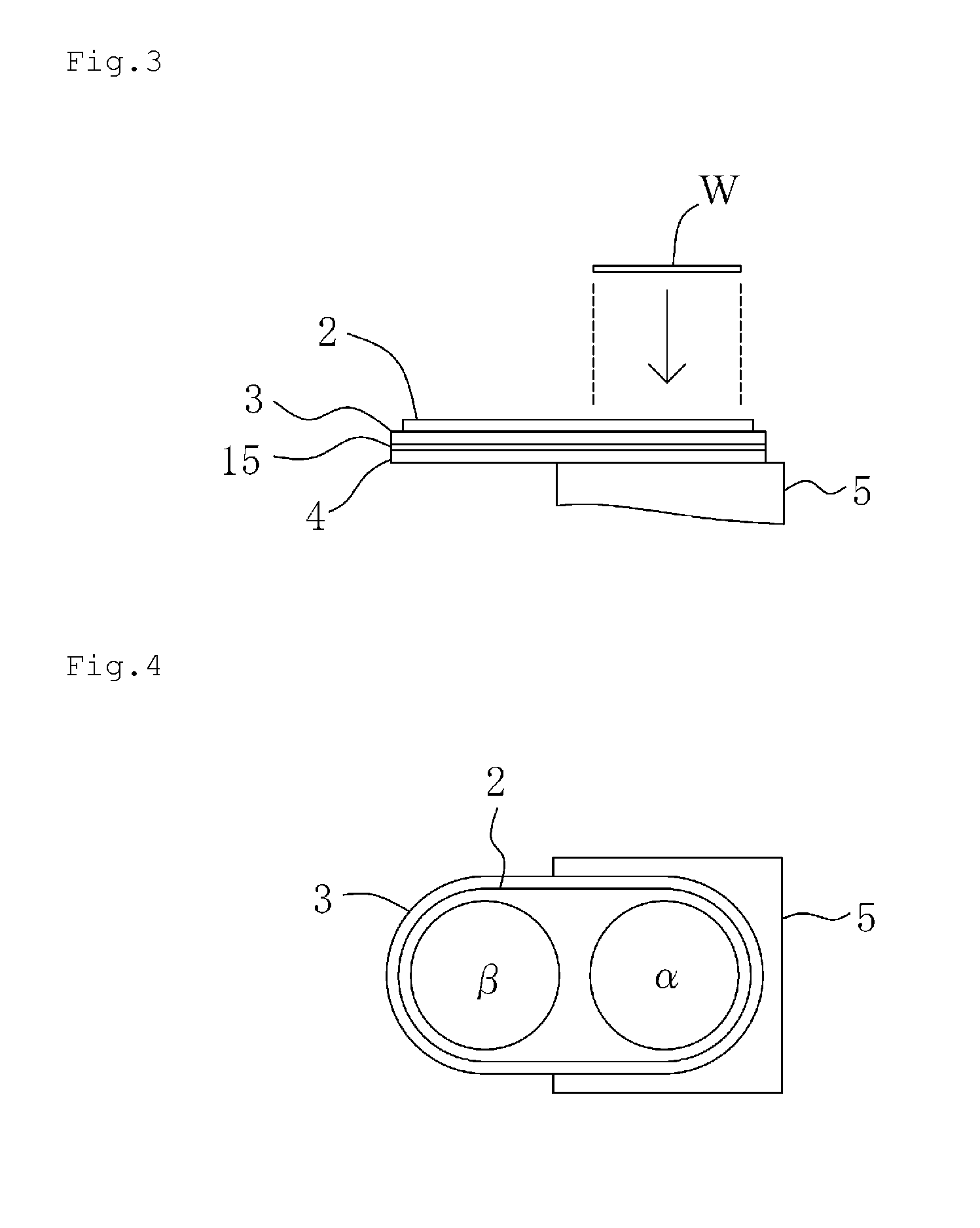
[0046]FIG. 1 is a partial cross section of a front view showing an example of an inspection apparatus for semiconductor devices according to the present invention. FIG. 2 is a plane view of the inspection apparatus as shown in FIG. 1. In FIG. 1 and FIG. 2, the reference numeral 1 indicates the inspection apparatus for semiconductor devices of the present invention. The reference numeral 2 indicates a chuck stage, the reference numeral 3 indicates an electric insulating plate on which the chuck stage 2 is p...
PUM
 Abstract
Description
Claims
Application Information