Substrate processing apparatus
- Summary
- Abstract
- Description
- Claims
- Application Information
AI Technical Summary
Benefits of technology
Problems solved by technology
Method used
Image
Examples
Embodiment Construction
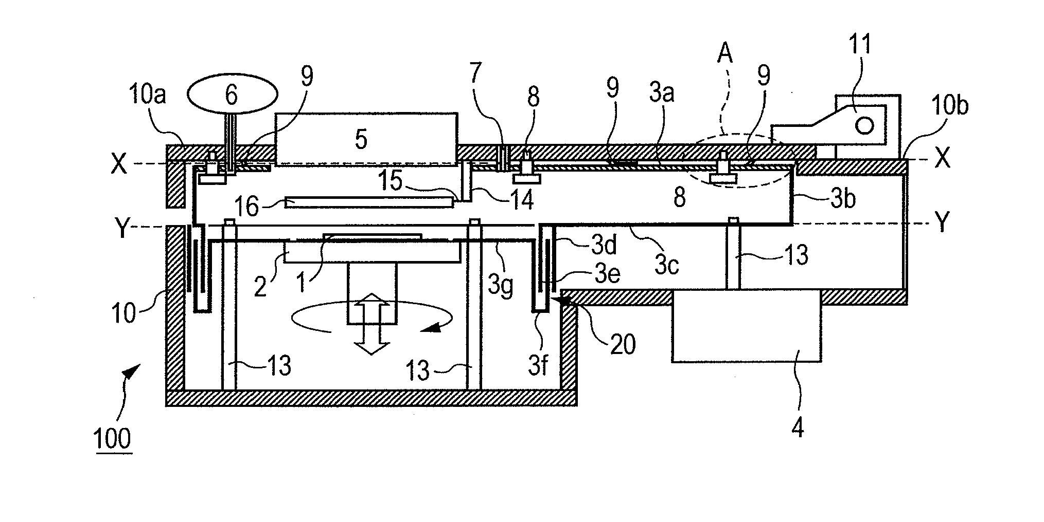
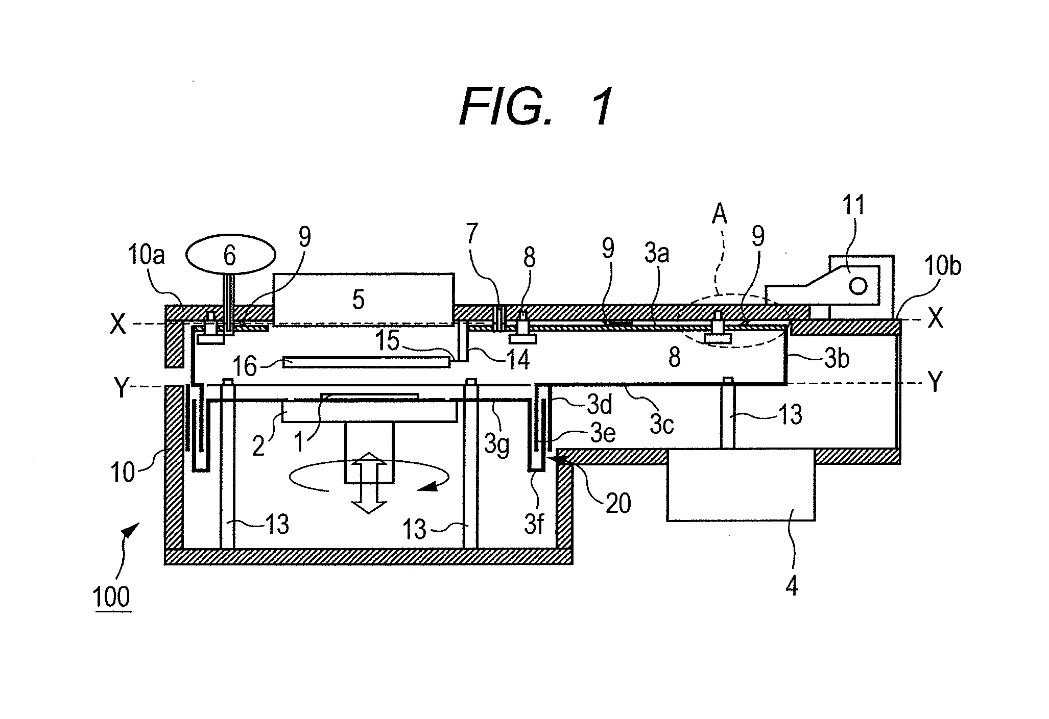
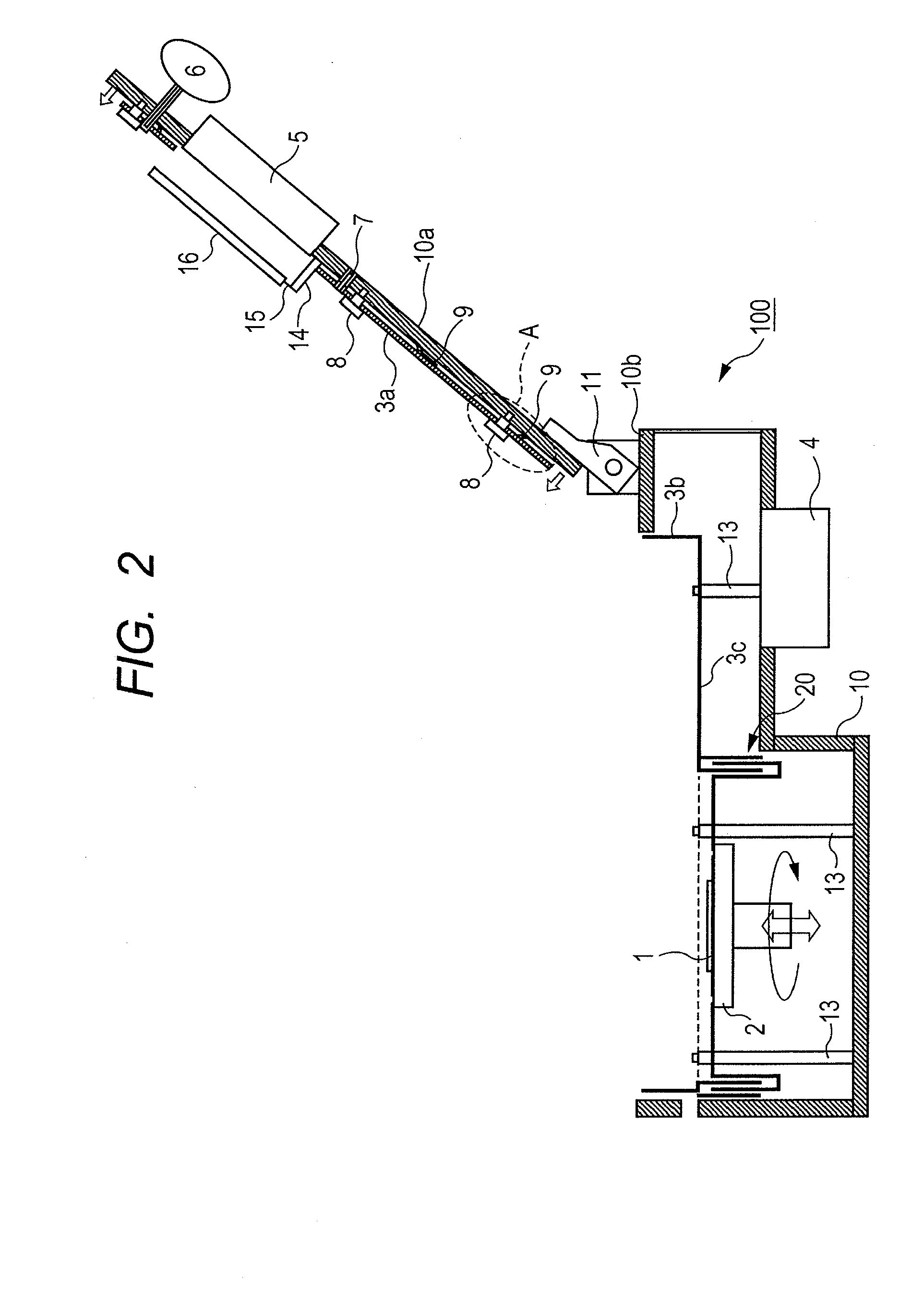
[0014]Hereinafter, a representative embodiment of the present invention will be described based on the accompanying drawings. FIGS. 1 and 2 are overall schematic diagrams of a substrate processing apparatus 100 according to one embodiment of the present invention. FIG. 1 shows a state where an opening of a chamber 10 is closed by a top lid 10a. FIG. 2 shows a state where the opening is opened. FIG. 3 is a top view of the cross section X-X in FIG. 1, seen from the above. In this embodiment, as an example of the substrate processing apparatus 100, description will be given of a sputtering apparatus used to produce magnetic sensors such as a read head for storage of a hard disk drive and for spintronics applications such as a non-volatile magnetoresistive random-access memory (MRAM). However, the gist of the present invention is not limited thereto. The present invention is applicable to, for example, vacuum processing systems such as a PVD system, a CVD system, and an etching system.
[...
PUM
| Property | Measurement | Unit |
|---|---|---|
| Distance | aaaaa | aaaaa |
Abstract
Description
Claims
Application Information


