Sample observing device and sample observing method

a sample observing and sample technology, applied in material analysis using wave/particle radiation, instruments, nuclear engineering, etc., can solve the problems of limiting the maximum scanning speed and not being able to increase the scanning speed more, so as to reduce the observation required time, increase the amount of secondary electrons, and increase the scanning speed

Active Publication Date: 2013-06-27
EBARA CORP
View PDF10 Cites 23 Cited by
  • Summary
  • Abstract
  • Description
  • Claims
  • Application Information

AI Technical Summary

Benefits of technology

[0008]It may be possible to increase a scanning speed in order to reduce an observation required time. Meanwhile, image quality of an observation image depends on the amount of the secondary electrons and the like, and therefore it is necessary to increase the amount of secondary electrons and the like to be detected per unit time in order to increase the scanning speed without decreasing image quality and therefore it is necessary to increase the amount of electrons to be irradiated with (increase a current).
[0009]However, the electron beam has property that, when there are a lot of electrons in the single space, electrons repel against each other due to a Coulomb effect resulting from negative electric charges of these electrons, and the electron beam widens (space-charge effect). Further, the electron beam widens more when an accelerating voltage is lower. Hence, when the resolution (that is, the diameter of the electron beam) is determined, a maximum value of the current is principally limited, resulting in limiting a maximum scanning speed, and therefore it is not possible to increase the scanning speed more.
[0010]The present invention is made in light of the above problem, and an object of the present invention is to provide a sample observing device and method which can have high resolution and reduce the time required to scan electron beams upon scanning the electron beams and observing the sample.

Problems solved by technology

Hence, when the resolution (that is, the diameter of the electron beam) is determined, a maximum value of the current is principally limited, resulting in limiting a maximum scanning speed, and therefore it is not possible to increase the scanning speed more.

Method used


Image

  • Sample observing device and sample observing method
  • Sample observing device and sample observing method
  • Sample observing device and sample observing method

Examples


Embodiment Construction

[0062]Hereinafter, the present invention will be described in detail. Embodiments described below are only examples of the present invention, and the present invention can be modified to various modes. Hence, specific configurations and functions disclosed below by no means limit the scope of the claims.

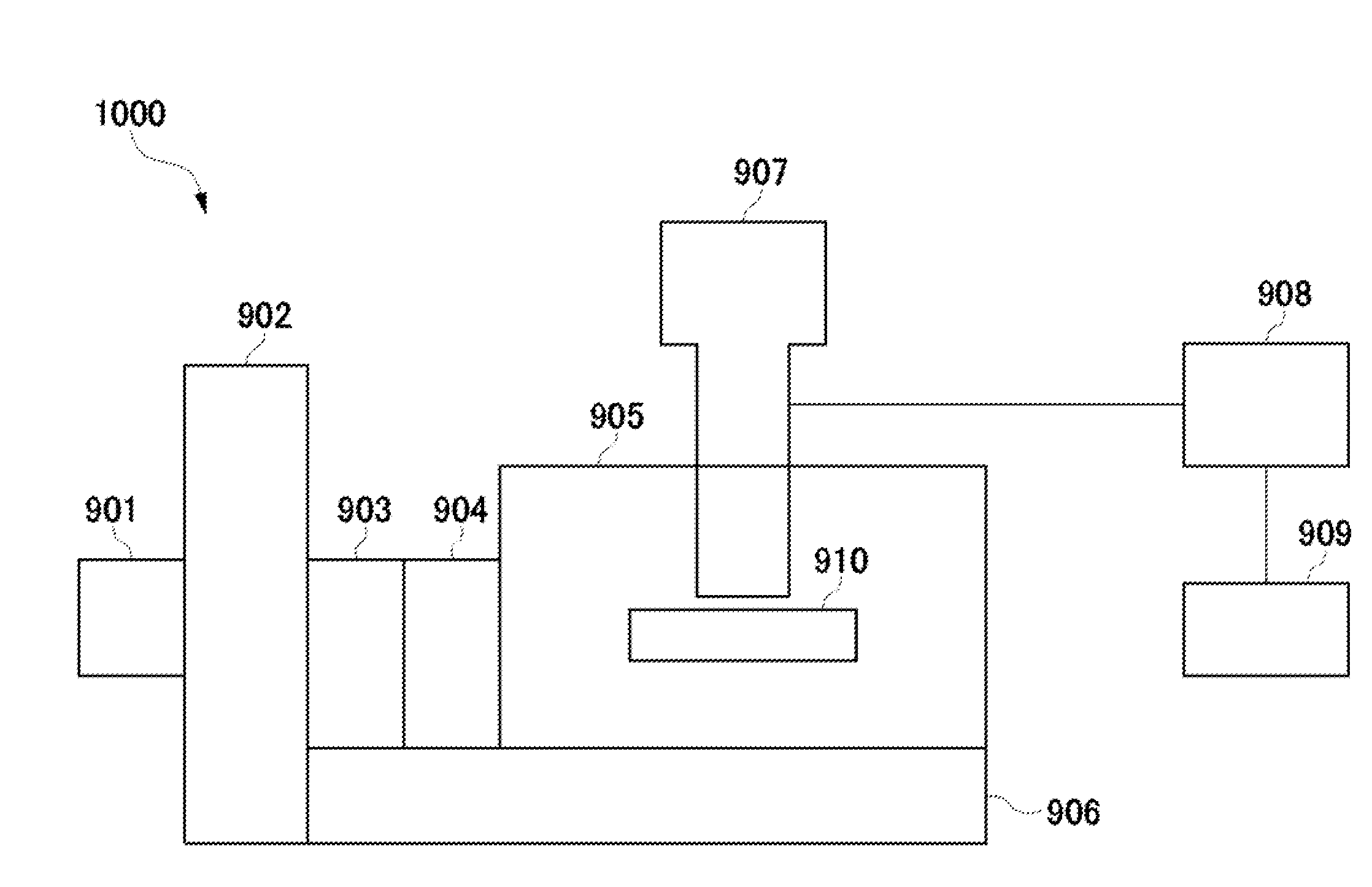
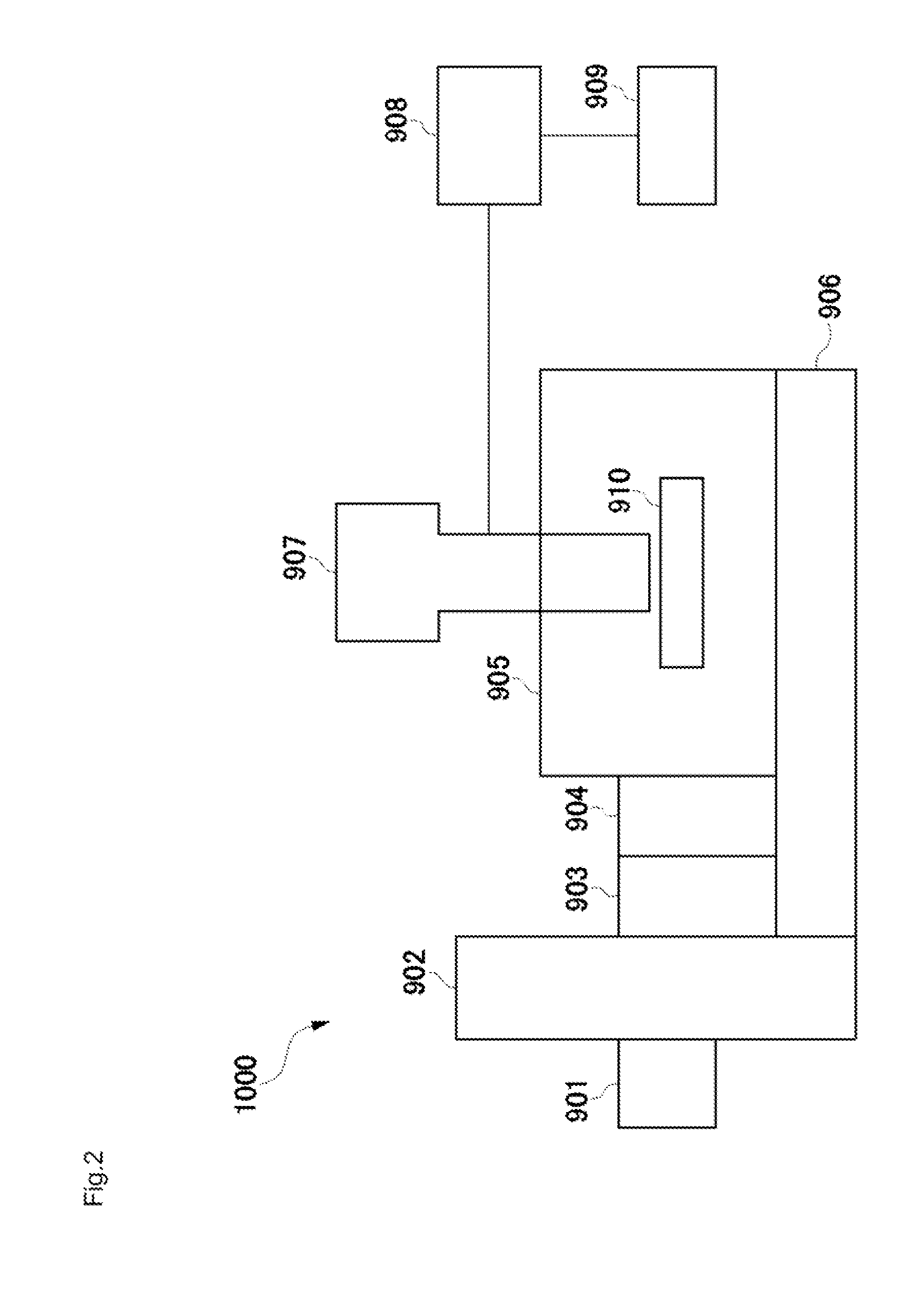
[0063]A sample observing device according to an embodiment of the present invention is a sample observing device which observes a sample by irradiating the sample set on a stage with an electron beam and detecting the electron beam from the sample, and has: an electron column which irradiates the sample with the electron beam and detects the electron beam from the sample, and the electron column has a plurality of electron beam irradiation detecting systems which each form an electron beam path in which the electron beam with which the sample is irradiated and the electron beam from the sample pass, and observes the sample by simultaneously using the plurality of electron beam irradi...


PUM


Abstract

An electron beam inspection device observes a sample by irradiating the sample set on a stage with electron beams and detecting the electron beams from the sample. The electron beam inspection device has one electron column which irradiates the sample with the electron beams, and detects the electron beams from the sample. In this one electron column, a plurality of electron beam irradiation detecting systems are formed which each form electron beam paths in which the electron beams with which the sample is irradiated and the electron beams from the sample pass. The electron beam inspection device inspects the sample by simultaneously using a plurality of electron beam irradiation detecting systems and simultaneously irradiating the sample with the plurality of electron beams.

Description

CROSS-REFERENCE TO RELATED APPLICATIONS[0001]This application claims priority to Japanese Patent No. 2011-236586 filed on Oct. 28, 2011, the entire contents of which are incorporated by reference herein.BACKGROUND OF THE INVENTION[0002]1. Field of the Invention[0003]The present invention relates to a sample observing device and a sample observing method which observe a sample by irradiating the sample with electron beams and detecting the electron beams from the sample.[0004]2. Description of Related Art[0005]Conventionally, in, for example, a field of semiconductor manufacturing, sample observing devices are used to, for example, inspect defects of sample substrates such as wafers and masks. In recent years, accompanying improvement in the degree of integration of semiconductor large-scale integrated circuits (LSI), patterns formed on wafers and masks are increasingly miniaturized, and, accompanying this miniaturization, sizes of defect detection targets are also becoming smaller. ...

Claims


Application Information

Patent Timeline
Patent Type & Authority Applications(United States)
IPC IPC(8): H01J37/26
CPCH01J37/261H01J37/073H01J37/12H01J37/265H01J37/28H01J2237/036H01J2237/2817H01J2237/06333H01J2237/1205H01J2237/1518H01J2237/186H01J2237/2443H01J2237/062G01N23/225H01J37/252
Inventor KARIMATA, TSUTOMUKOHAMA, TATSUYAYOSHIKAWA, SHOJIHATAKEYAMA, MASAHIRO
Owner EBARA CORP
Why Eureka
Try Eureka