Semiconductor device and method for manufacturing the same

a semiconductor device and semiconductor technology, applied in the direction of semiconductor devices, electrical devices, transistors, etc., can solve the problems of difficult to reduce off-state current sufficiently, and the switching characteristics may be degraded, so as to achieve the effect of controlling the deterioration of the semiconductor devi

Inactive Publication Date: 2013-06-27
SEMICON ENERGY LAB CO LTD
View PDF18 Cites 45 Cited by
  • Summary
  • Abstract
  • Description
  • Claims
  • Application Information

AI Technical Summary

Benefits of technology

[0013]With the use of the CAAC-OS, the change in electric characteristics of the transistor due to irradiation with visible light or ultraviolet light can be reduced; thus, the transistor can have high reliability.
[0062]According to one embodiment of the present invention, release of an oxygen atom from a side surface of an oxide semiconductor film can be prevented and the CAAC-OS can contain sufficient oxygen. Further, deterioration of the semiconductor device can be controlled.

Problems solved by technology

That is, when there are many oxygen vacancies in the oxide semiconductor film, conductivity becomes high, so that it becomes difficult to reduce off-state current sufficiently, and switching characteristics may be degraded.

Method used


Image

  • Semiconductor device and method for manufacturing the same
  • Semiconductor device and method for manufacturing the same
  • Semiconductor device and method for manufacturing the same

Examples


embodiment 1

[0077]In this embodiment, a semiconductor device (transistor) that is one embodiment of the present invention and a manufacturing method thereof are described.

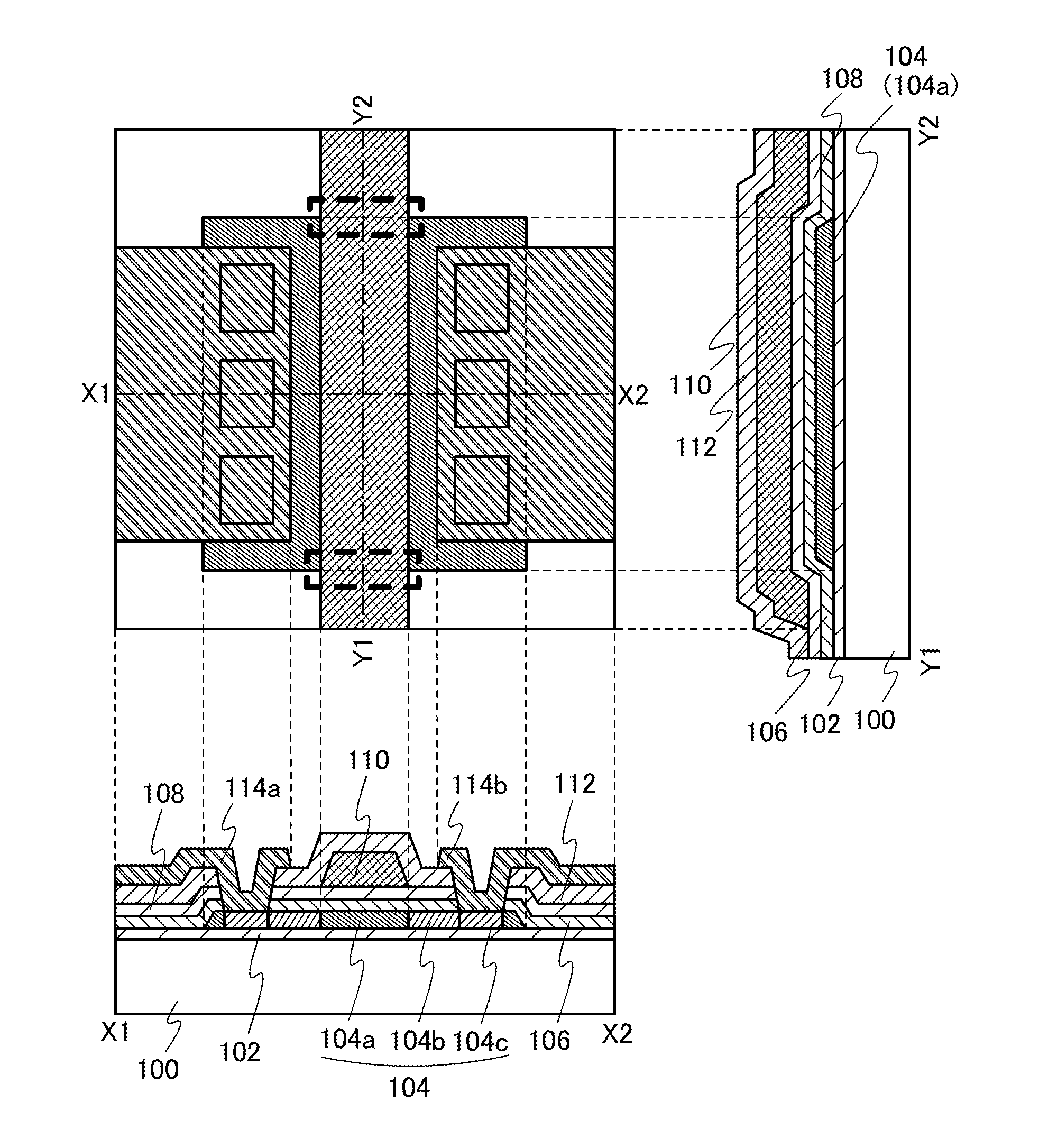
[0078]FIGS. 5A to 5C illustrate a transistor as a semiconductor device which is an embodiment of the present invention. FIG. 5A is a top view of the transistor. FIG. 5B is a cross-sectional view taken along the line X1-X2 in FIG. 5A, and FIG. 5C is a cross-sectional view taken along the line Y1-Y2 in FIG. 5A.

[0079]The transistor illustrated in FIGS. 5A to 5C includes a base film 102 provided over a substrate 100, an island-shaped oxide semiconductor film 104 provided over the base film 102, a first gate insulating film 106 provided to cover the island-shaped oxide semiconductor film 104, a second gate insulating film 108 provided over the first gate insulating film 106, a gate electrode 110 provided over the second gate insulating film 108, an interlayer insulating film 112 provided to cover the gate electrode 110, and a sourc...

embodiment 2

[0122]The semiconductor device described in Embodiment 1 which is one embodiment of the present invention can be provided in electronic devices. In this embodiment, an electronic device including the transistor described in Embodiment 1 is described.

[0123]FIGS. 9A and 9B illustrate a tablet terminal that can be folded. FIG. 9A illustrates the tablet terminal opened, and FIG. 9B illustrates the tablet terminal folded. The tablet terminal illustrated in FIG. 9A includes a housing 200, a display portion 202a, a display portion 202b, a clip 206, a display-mode switching button 208, a power button 210, a power-saving-mode switching button 212, and an operation button 214.

[0124]The semiconductor device in Embodiment 1 can be applied to pixel transistors in the display portions 202a and 202b. Alternatively, the semiconductor device in Embodiment 1 may be applied to a memory element of the tablet terminal illustrated in FIGS. 9A and 9B.

[0125]Further, part of the display portion 202a can be ...


PUM

PropertyMeasurementUnit
temperatureaaaaaaaaaa
energy barrieraaaaaaaaaa

Abstract

Release of oxygen at a side surface of an island-shaped oxide semiconductor film is controlled and decrease in resistance is prevented. A semiconductor device includes an island-shaped oxide semiconductor film at least partly including a crystal, a first gate insulating film provided to cover at least a side surface of the island-shaped oxide semiconductor film, and a second gate insulating film provided to cover at least the island-shaped oxide semiconductor film and the first gate insulating film. The first gate insulating film is an insulating film that supplies oxygen to the island-shaped oxide semiconductor film, and the second gate insulating film is an insulating film which has a low oxygen-transmitting property

Description

BACKGROUND OF THE INVENTION[0001]1. Field of the Invention[0002]The present invention relates to a semiconductor device and a method for manufacturing the semiconductor device.[0003]2. Description of the Related Art[0004]In recent years, metal oxides having semiconductor characteristics (hereinafter, referred to as oxide semiconductors) have attracted attention. An oxide semiconductor can be applied to a transistor (see Patent Documents 1 and 2).REFERENCEPatent Document[0005][Patent Document 1] Japanese Published Patent Application No. 2007-123861[0006][Patent Document 2] Japanese Published Patent Application No. 2007-096055SUMMARY OF THE INVENTION[0007]Oxygen vacancy significantly influences electric characteristics of a transistor which includes an oxide semiconductor. That is, when there are many oxygen vacancies in the oxide semiconductor film, conductivity becomes high, so that it becomes difficult to reduce off-state current sufficiently, and switching characteristics may be d...

Claims


Application Information

Patent Timeline
Patent Type & Authority Applications(United States)
IPC IPC(8): H01L29/786H01L21/36
CPCH01L29/786H01L29/7869H01L29/4908H01L21/36
Inventor YAMAZAKI, SHUNPEIMATSUBAYASHI, DAISUKEISOBE, ATSUO
Owner SEMICON ENERGY LAB CO LTD
Why Eureka
Try Eureka