Zero shrinkage smooth interface oxy-nitride and oxy-amorphous-silicon stacks for 3D memory vertical gate application

a technology of oxy-nitride and oxy-amorphous silicon, applied in the direction of solid-state devices, coatings, chemical vapor deposition coatings, etc., can solve the problems of different materials that undergo volume change at different rates, limit the creation of high-capacity devices on a small scale, and achieve the effect of reducing alfx accumulation and reducing alfx building up

Inactive Publication Date: 2013-06-27
APPLIED MATERIALS INC
View PDF3 Cites 334 Cited by
  • Summary
  • Abstract
  • Description
  • Claims
  • Application Information

AI Technical Summary

Benefits of technology

[0011]In a further embodiment, the nitride and oxide deposition temperatures are about 600° C. or greater. In a still further embodiment, a showerhead having a straight hole faceplate is used for supplying the process gases into the processing chamber. In additional embodiments, the method provides for coating at least a portion of the deposition reactor with yttrium oxide to reduce AlFx deposits during subsequent cleaning operations. In other embodiments, the sacrificial nitride film layers are silicon nitride and the oxide film layers are silicon oxide.
[0012]In addition, the one or more process gases used to deposit silicon nitride layers comprise silane and ammonia, and the ammonia exceeds the silane on a volumetric basis. Other embodiments provide that the ammonia is at least 100 times as much as the silane, on a volumetric basis. In further embodiments, the one or more process gases used to deposit silicon nitride layers further comprises molecular nitrogen. In additional embodiments, the process gases used to deposit silicon nitride and the process gases used to deposit silicon oxide further comprise one or more dilution gases that are inert at process conditions. In another embodiment, the one or more dilution gases is argon and/or helium. Other embodiments provide that the one or more process gases used to deposit silicon oxide comprise tetraethoxysilane, N2O and a dilution gas that is inert at process conditions.
[0013]Another embodiment provides for a method for depositing a stack of film layers for use in vertical gates for 3D memory devices, the method comprising supplying one or more process gases suitable for depositing an amorphous silicon film into a processing chamber of a deposition reactor, depositing an amorphous silicon film layer at an amorphous silicon film deposition temperature greater than about 550° C., supplying one or more process gases suitable for depositing a silicon oxide film into a processing chamber of a deposition reactor, depositing an oxide film layer over the nitride film layer, at a silicon oxide deposition temperature greater than about 550° C., repeating the above steps to deposit a film stack having alternating layers of the amorphous silicon films and the silicon oxide films, forming a plurality of holes in the film stack, and depositing polysilicon in the plurality of holes in the film stack at a polysilicon process temperature of about 700° C. or greater, w...

Problems solved by technology

However, as flash technology has progressed, limitations exist in how to create high capacity devices on a small scale.
For example, different materials that are combined on a microscopic scale have different physical properties that lead to non-uniformities in a flash memory device.
Further, high heat process steps can cause the different materials to undergo volume changes at different rates.
These problems can cause a deposited stack of different layers to warp.
Warping problems limit the number of layers tha...

Method used


Image

  • Zero shrinkage smooth interface oxy-nitride and oxy-amorphous-silicon stacks for 3D memory vertical gate application
  • Zero shrinkage smooth interface oxy-nitride and oxy-amorphous-silicon stacks for 3D memory vertical gate application
  • Zero shrinkage smooth interface oxy-nitride and oxy-amorphous-silicon stacks for 3D memory vertical gate application

Examples


Embodiment Construction

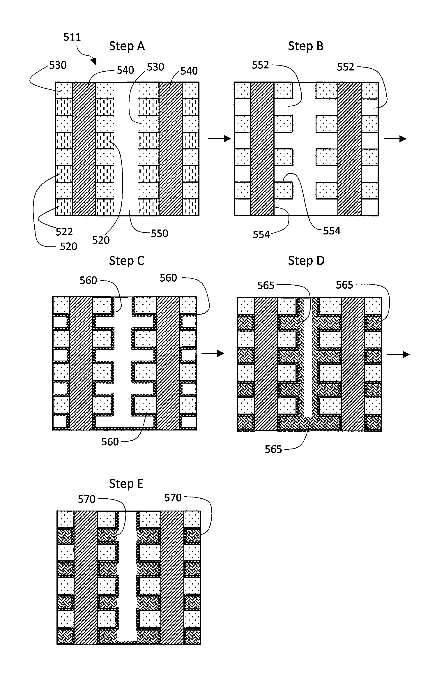
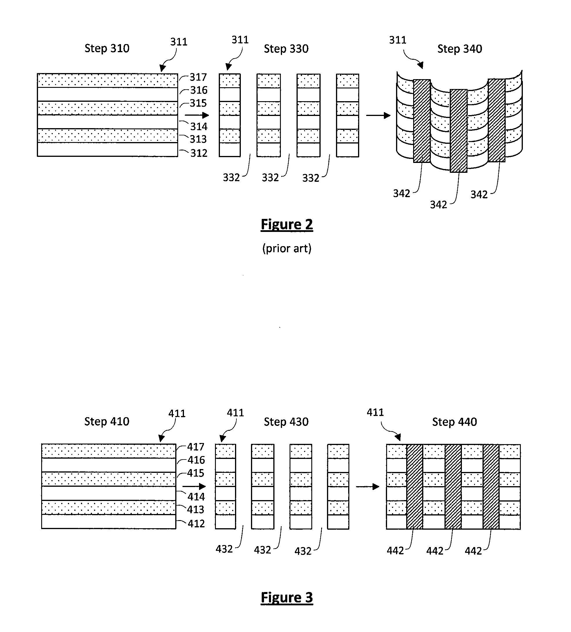
[0023]Embodiments discussed herein provide for improved stacks for 3D memory devices, methods for producing 3D memory devices and apparatuses for producing 3D memory devices. Further embodiments are described for approaches to reduce and / or eliminate shrinkage in alternating film layers in a stack when those layers are exposed to a high temperature process such as an anneal.

[0024]In order to micronize memory cells in vertical 3D arrangements, film layers are deposited into a stack, which is then further processed to create arrays of string cells. Some examples discussed herein relate to a Terabit Cell Array Transistor (TCAT) flash memory structure, in which a cell string has six-NAND cell transistors. But it is to be understood that the ideas disclosed herein may be applied to other 3D or vertical gate memory structures as well. For example, other configurations may use three-dimensional Bit-Cost Scalable (BiCS) flash memory. Other flash memory devices may use pipe-shaped Bit Cost S...


PUM

PropertyMeasurementUnit
Temperatureaaaaaaaaaa

Abstract

Methods are provided for depositing a stack of film layers for use in vertical gates for 3D memory devices, by depositing a sacrificial nitride film layer at a sacrificial film deposition temperature greater than about 550° C.; depositing an oxide film layer over the nitride film layer, at an oxide deposition temperature of about 600° C. or greater; repeating the above steps to deposit a film stack having alternating layers of the sacrificial films and the oxide films; forming a plurality of holes in the film stack; and depositing polysilicon in the plurality of holes in the film stack at a polysilicon process temperature of about 700° C. or greater, wherein the sacrificial film layers and the oxide film layers experience near zero shrinkage during the polysilicon deposition. Flash drive memory devices may also be made by these methods.

Description

BACKGROUND OF THE INVENTION[0001]1. Field of the Invention[0002]Aspects of the present invention generally relate to methods and devices for stacks in 3D memory vertical gate applications. Further aspects relate to low or zero shrinkage stacks achieved from smooth interfaces between alternating layers of oxide and nitride films or oxide and amorphous silicon films.[0003]2. Description of the Related Art[0004]Computer memory devices are ever in pursuit of smaller geometries with increased capacity at less cost. To this end, components of memory cells are stacked on top of each other to create 3D cells. One such technology is NAND flash memory, which may be found in memory cards, USB flash drives, solid-state drives and similar products, for data storage and transfer. In NAND flash memory, memory cells made from transistors are connected in series, and can be stacked into vertical layers to create densely packed, high capacity devices. With no moving parts, flash drives use less power...

Claims


Application Information

Patent Timeline
IPC IPC(8): H01L29/78H01L21/20
CPCH01L29/66833H01L29/7926H01L27/11582C23C16/24C23C16/345H01L21/02274C23C16/505H01L21/02164H01L21/0217H01L21/022C23C16/401H10B43/27
Inventor HAN, XINHAIRAJAGOPALAN, NAGARAJANXUAN, GUANGCHIZHOU, JIANHUALI, JIGANGSHAIKH, SHAHIDREILLY, PATRICKNOWAK, THOMASROCHA-ALVAREZ, JUAN CARLOSPARK, HEUNG LAKKIM, BOK HOEN
Owner APPLIED MATERIALS INC
Why Eureka
Try Eureka