
Memory circuit incorporating radiation-hardened memory scrub engine

a memory scrub engine and memory circuit technology, applied in the field of integrated circuits, can solve the problems of increasing the risk of individual bit errors, significantly affecting the reliability of the electronic control system, etc., and achieves the effect of achieving acceptable (error-free) reliable operation and nearly impossibl

Active Publication Date: 2013-06-27
SILICON SPACE TECH
View PDF3 Cites 15 Cited by
  • Summary
  • Abstract
  • Description
  • Claims
  • Application Information

AI Technical Summary

Benefits of technology

The patent describes an integrated circuit that includes two memory arrays and corresponding error detection and correction circuits. The error detection and correction circuits include spatially redundant circuitry, such as DICE circuits or temporal filtering circuitry, to detect and correct errors in data groups read from the memory arrays. The integrated circuit also includes an output circuit to present the data groups as a single addressable data group or separately addressable data groups. The technical effect of the invention is to improve the accuracy and reliability of the integrated circuit by detecting and correcting errors in data groups read from the memory arrays.

Problems solved by technology

Certain extreme environments (where CMOS circuits need to operate) exist which will significantly increase the risk for individual bit errors, which in turn can significantly affect the reliability of the electronic control system.
However, for CMOS circuits which operate in extreme environments, the FIT rates are dramatically increased to the extent that acceptable (error-free) reliable operation becomes nearly impossible.

Method used


Image

  • Memory circuit incorporating radiation-hardened memory scrub engine
  • Memory circuit incorporating radiation-hardened memory scrub engine
  • Memory circuit incorporating radiation-hardened memory scrub engine

Examples


example dice

Cells

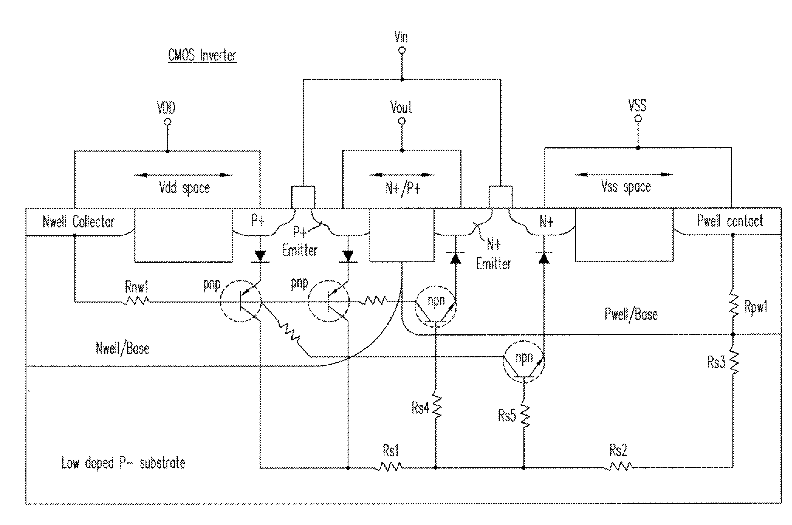
[0101]In an example SRAM embodiment, both BGR techniques and DICE cells are implemented. Versions of the DICE structure can be used to replace memory cells, flip-flops, and latches, but they generally require twice the number of transistors compared to the standard, non-radiation-hard versions. This is more area-efficient than triple-modular redundancy (TMR), which takes about three times the area and also requires an additional voting stage. In standard usage, the DICE cell generally provides improved SEE performance. However, L. W. Massengill et al., in “Single Event Mechanisms Impacting Sub-100 nm Radiation-Hardened Design,” (presented at GOMAC Conference, March 2007) and others have shown that most DICE parts still fail above a LET threshold around 30 to 40 MeV / (mg / cm2) including some with thresholds less than 5 MeV / (mg / cm2). The problem with standard DICE is related to the parasitic bipolar transistors that get turned on during a SEE event. The induced currents can often t...


PUM


Abstract

An example integrated circuit includes a first memory array including a first plurality of data groups, each such data group including a respective plurality of data bits. The integrated circuit also includes a first error detection and correction (EDAC) circuit configured to detect and correct an error in a data group read from the first memory array. The integrated circuit also includes a first scrub circuit configured to access in a sequence each of the first plurality of data groups to correct any detected errors therein. Both the first EDAC circuit and the first scrub circuit include spatially redundant circuitry. The first EDAC circuit and the first scrub circuit may include buried guard ring (BGR) structures, and may include parasitic isolation device (PID) structures. The spatially redundant circuitry may include dual interlocked storage cell (DICE) circuits, and may include temporal filtering circuitry.

Description

CROSS-REFERENCE TO RELATED APPLICATION(S)[0001]This application claims the benefit under 35 U.S.C. §119(e) of U.S. Provisional Application No. 61 / 562,647, filed Nov. 22, 2011, entitled “Reliability Improvement Using Spatially-Redundant Circuits, EDAC, and Memory Scrub” by Wesley H. Morris, Robert Fuller, David Gifford, Rex Lowther, and Jon Gwin, which application is hereby incorporated by reference.MASK WORK NOTICE[0002]A portion of the disclosure of this patent document contains material which is subject to mask work protection. The mask work owner has no objection to the facsimile reproduction by anyone of the patent document or the patent disclosure, as it appears in the U.S. Patent and Trademark Office patent file or records, but otherwise reserves all mask work rights whatsoever.BACKGROUND[0003]1. Field of the Invention[0004]The present invention relates to integrated circuits, and particularly to integrated circuits with partial and / or complete immunity to failure modes associ...

Claims


Application Information

Patent Timeline
IPC IPC(8): G06F11/07H03K19/003G11C8/00
CPCG06F11/183G06F11/0793G06F11/186H03K19/00392G06F11/1048G11C8/00G06F11/1008
Inventor MORRIS, WESLEY H.GIFFORD, DAVID R.LOWTHER, REX E.
Owner SILICON SPACE TECH
Learn More