
Silicon Carbide Schottky Diode Device with Mesa Termination and Manufacturing Method Thereof

a technology of silicon carbide schottky diodes and diodes, which is applied in the direction of semiconductor devices, basic electric elements, electrical apparatus, etc., can solve the problems of non-uniform depletion region and limitation of the operation of conventional schottky diodes, and achieve the effect of higher voltag

Inactive Publication Date: 2013-07-04
NAT TAIWAN UNIV
View PDF0 Cites 6 Cited by
  • Summary
  • Abstract
  • Description
  • Claims
  • Application Information

AI Technical Summary

Benefits of technology

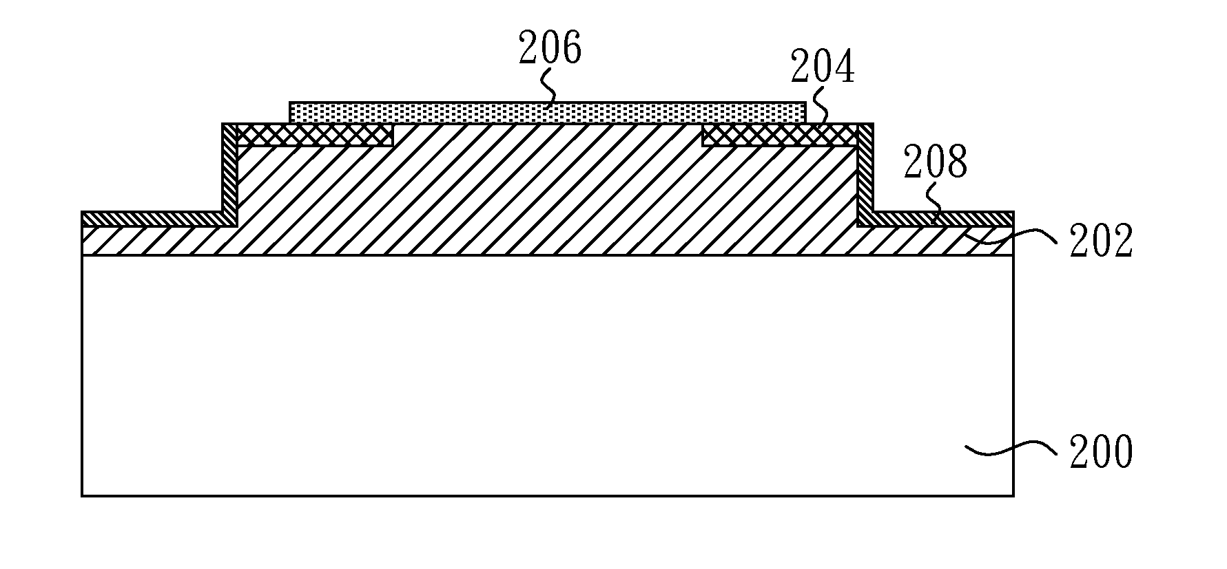
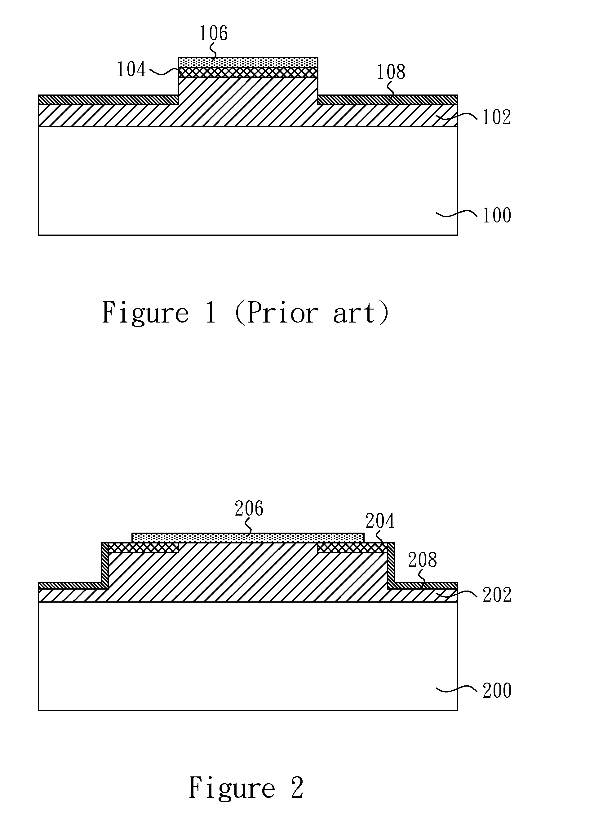
The invention provides a Schottky diode device with mesa terminations that can withstand higher voltages when a bias voltage is applied. This is achieved by extending the junction termination extension structure with mesas, which prevents the depletion region in the n-type semiconductor layer from extending laterally and allows the device to achieve a higher breakdown voltage. Additionally, the device has a larger on-state current or a smaller on-state resistance and requires less production cost compared to conventional devices. The invention's junction termination extension structure with mesas has a larger breakdown voltage compared to conventional devices as the depletion region is confined in the central region of the n-type semiconductor layer.

Problems solved by technology

The surface effect may cause a non-uniform depletion region so as to affect the breakdown voltage of the device.
That is, the conventional Schottky diode device shown in FIG. 1 would not be able to sustain a higher voltage without being breakdown when a bias voltage is applied and thus such feature constitutes a limitation for the operation of the conventional Schottky diode device.

Method used


Image

  • Silicon Carbide Schottky Diode Device with Mesa Termination and Manufacturing Method Thereof
  • Silicon Carbide Schottky Diode Device with Mesa Termination and Manufacturing Method Thereof
  • Silicon Carbide Schottky Diode Device with Mesa Termination and Manufacturing Method Thereof

Examples


Embodiment Construction

[0020]Various example embodiments of the present invention will now be described more fully with reference to the accompanying drawings in which some example embodiments of the invention are shown. In the drawings, the size of every component may be exaggerated for clarity. Detailed illustrative embodiments of the present invention are disclosed herein. However, specific structural and functional details disclosed herein are merely representative for purposes of describing example embodiments of the present invention. This invention may, however, be embodied in many alternate forms and should not be construed as limited to only the embodiments set forth herein.

[0021]Accordingly, while example embodiments of the invention are capable of various modifications and alternative forms, embodiments thereof are shown by way of example in the drawings and will herein be described in detail. It should be understood, however, that there is no intent to limit example embodiments of the inventio...


PUM


Abstract

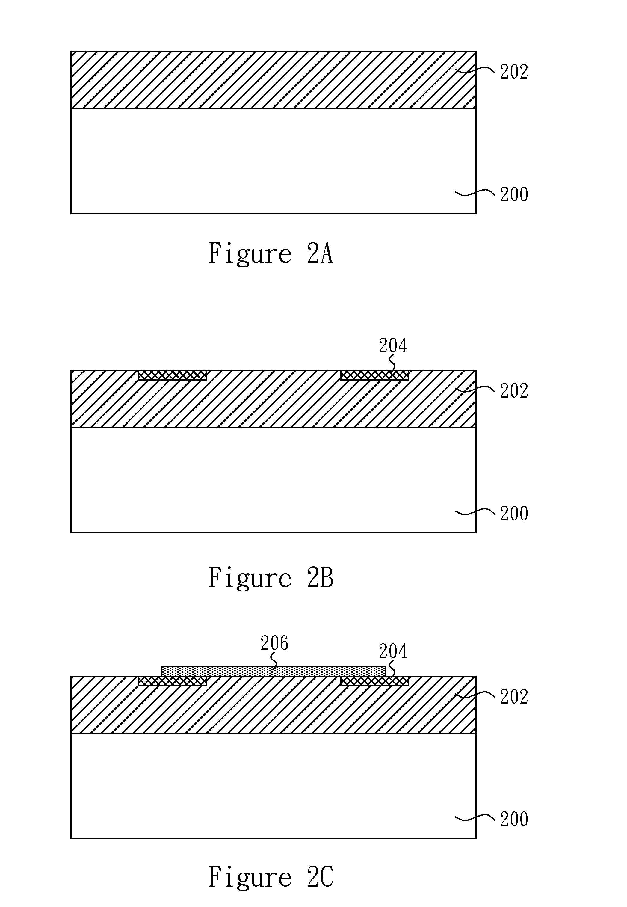
A silicon carbide Schottky diode device with mesa terminations and the manufacturing method thereof are provided. The silicon carbide Schottky diode device includes an n-type epitaxial silicon carbide layer with mesa terminations on an n-type silicon carbide substrate, two p-type regions in the n-type epitaxial silicon carbide layer and a Schottky metal contact on the n-type epitaxial silicon carbide layer and the p-type regions, a dielectric layer on sidewalls and planes of the mesa terminations.

Description

CROSS-REFERENCE TO RELATED APPLICATIONS[0001]The entire contents of Taiwan Patent Application No. 101100349, filed on Jan. 4, 2012, from which this application claims priority, are incorporated herein by reference.BACKGROUND OF THE INVENTION[0002]1. Field of the Invention[0003]The present invention relates to a diode device and the manufacturing method thereof, and more particularly to a silicon carbide Schottky diode device with mesa terminations and the manufacturing method thereof.[0004]2. Description of Related Art[0005]Conventional silicon carbide Schottky diode device usually consists of an n-type silicon carbide substrate and an n-type epitaxial silicon carbide layer. Conventional silicon carbide Schottky diode device further consists of Schottky metal contacts formed directly on the n-type epitaxial silicon carbide layer. The Schottky metal contacts are further surrounded by a p-type junction termination extension (JTE) region formed by an ion implantation process. The junct...

Claims


Application Information

Patent Timeline
IPC IPC(8): H01L29/161H01L21/329
CPCH01L29/66143H01L29/2003H01L29/872H01L29/861
Inventor WANG, HUI-HSUANHUANG, HAO-CHENLIU, CHEE-WEE
Owner NAT TAIWAN UNIV
Learn More