Nanowire enhanced transparent conductive oxide for thin film photovoltaic devices

a technology of transparent conductive oxide and nanowires, which is applied in the field of nanowire enhanced transparent conductive oxide for thin film photovoltaic devices, can solve the problems of tens of microns range, conductive wire size, and past techniques, and achieve high conductivity materials, facilitate scattering of incident electromagnetic radiation, and high efficiency

Inactive Publication Date: 2013-07-11
CM MFG
View PDF3 Cites 17 Cited by
  • Summary
  • Abstract
  • Description
  • Claims
  • Application Information

AI Technical Summary

Benefits of technology

[0007]In an alternative embodiment the method includes applying nanowire structures over the upper surface with a coverage of about 1% and greater. A transparent conductor material is formed over the nanowires to embed them in the transparent conductor material. The nanowires structures facilitate scattering of incident electromagnetic radiation while allowing the electromagnetic radiation to traverse the thickness of the transparent conductor material and yet not block the absorber material.
[0008]The method and structure provided are incorporated in a series of innovative manufacturing processes for making next generation high efficiency thin-film photovoltaic devices. In various embodiments, an nanowire-enhanced transparent conductive oxide film is formed by first adding a TCO film followed by embedding nanowires on the TCO film or simultaneously adding conductive nanowires and forming TCO film. The nanowires are configured in substantially random patterns with about 1% or more physical coverage in the surface area subjected to incoming light. The nanowires are made by high conductivity material, for example, copper, silver or metal alloys, although carbon or organic material can be also be used. In one embodiment, the nanowires are 100 nm or less in diameter with a random crossing configuration, a structure that facilitates off-resonance scattering of electromagnetic waves on the nanowires via surface Plasmon effects and causes substantially no absorption loss of the incoming light. In addition to the small geometric shadowing area of the nanowires, the scattering effect reduces the cross section area blocking light into the absorber material and enables using a host TCO film with substantially lower doping than non-nanowire-enhanced TCO film. As the result, the nanowire-enhanced TCO film has an enhanced lateral conductivity and carrier mobility so that the device can capture more light-converted current with improved efficiency.

Problems solved by technology

While conventional techniques in the past have addressed some of these issues, they are often inadequate.
The size of the conductive wires, however, is in tens of microns range which is still relatively large and difficult in practice to achieve a reduction in resistance without causing the absorption of incoming light by the added wires.

Method used


Image

  • Nanowire enhanced transparent conductive oxide for thin film photovoltaic devices
  • Nanowire enhanced transparent conductive oxide for thin film photovoltaic devices
  • Nanowire enhanced transparent conductive oxide for thin film photovoltaic devices

Examples


Embodiment Construction

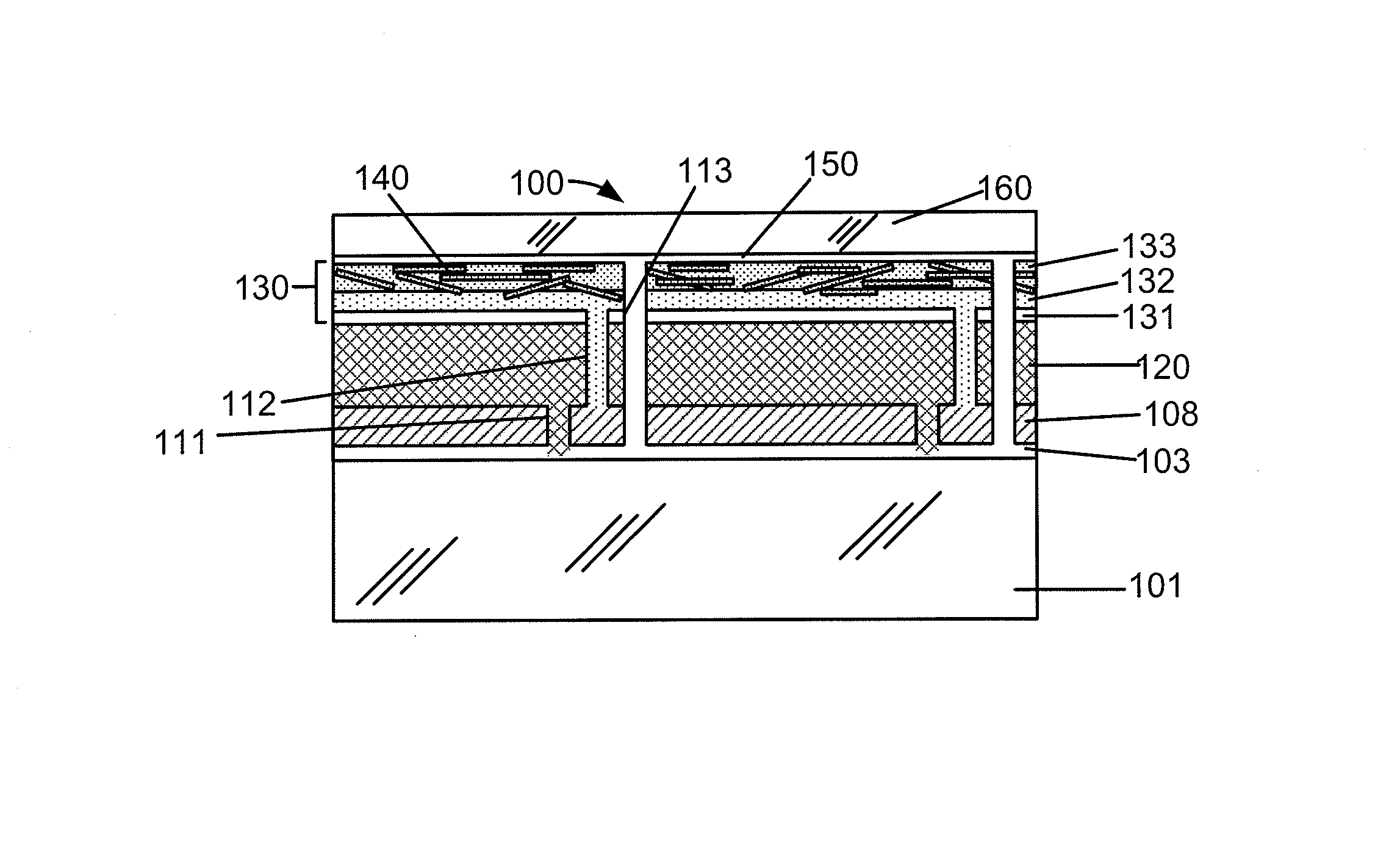
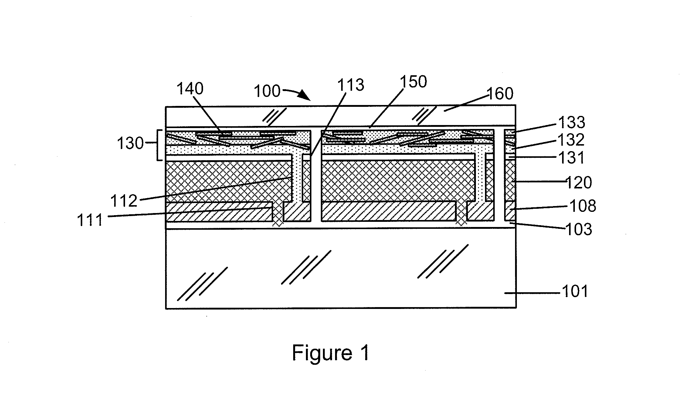
[0020]FIG. 1 is a cross-section view of a thin-film photovoltaic device with a nanowire-enhanced transparent conductive oxide (TCO) film according to an embodiment of the invention. The thin-film photovoltaic device 100 is formed through thin-film manufacturing processes including forming a nanowire-enhanced optically transparent conductive electrode over the photovoltaic absorber material. As shown, the thin-film photovoltaic device 100 includes cells patterned from a series of continuous thin films formed on a substrate structure 101, including at least a barrier later 103, a bottom electrode 110, an absorber material 120, a top electrode 130, and a cap glass 160. As known, transparent conductive oxide (TCO) material is widely used for forming a thin-film electrode as the top electrode of a photovoltaic cell. By incorporation of high conductivity nanowires into the TCO film, enhancement of lateral conductivity without appreciable reduction in optical transmission is achieved.

[0021...


PUM

PropertyMeasurementUnit
transparentaaaaaaaaaa
sheet resistivityaaaaaaaaaa
optical transparencyaaaaaaaaaa

Abstract

A thin-film photovoltaic devices includes transparent conductive oxide which has embedded within it nanowires at less than 2% nominal shadowing area. The nanowires enhance the electrical conductivity of the conductive oxide.

Description

CROSS-REFERENCES TO RELATED APPLICATIONS[0001]This application claims the benefit of U.S. Provisional Application No. 61 / 505,475, filed Jul. 7, 2011, entitled “Nanowire Enhanced Transparent Conductive Oxide for Thin Film Photovoltaic Devices.” The entire disclosure of which is incorporated herein by reference for all purposes.BACKGROUND OF THE INVENTION[0002]This invention relates generally to thin-film photovoltaic techniques and more particularly, to a method and structure of a nanowire-enhanced transparent conductive film for thin-film photovoltaic devices. Embodiments of the present invention can be applied to embed metallic nanowires in a transparent conductive oxide film for the manufacture of thin-film photovoltaic devices.[0003]In the process of manufacturing thin-film photovoltaic devices based on copper-indium-selenium (CIS) and / or copper-indium-gallium-selenium (CIGS) absorber materials, there are various manufacturing challenges, such as scaling up the manufacturing to l...

Claims


Application Information

Patent Timeline
Patent Type & Authority Applications(United States)
IPC IPC(8): H01L31/18H01L31/0224
CPCH01L31/1884H01L31/022466Y02E10/541B82Y10/00H01L31/0749B82Y99/00Y02P70/50
Inventor FARRIS, III, CHESTER A.WIETING, ROBERT D.TANDON, ASHISH
Owner CM MFG
Why Eureka
Try Eureka