Serial thermal linear processor arrangement

a linear processor and linear technology, applied in the field of electrical components, can solve the problems of reducing the reliability of the device produced, the flux cannot be completely cleaned between the die and the substrate, and the mechanical system for delivering the chemical is easy and controllable, and the system requirements are much higher

Inactive Publication Date: 2013-07-11
SEMLGEAR INC
View PDF7 Cites 23 Cited by
  • Summary
  • Abstract
  • Description
  • Claims
  • Application Information

AI Technical Summary

Benefits of technology

[0038]By using a stepped, independent, multi-chamber linearly aligned machine such as utilized with the present invention, removal of moisture on the surface can be easily accomplished. Removal of surface oxides or the minimization of voids inside the solder bumps or balls may be accomplished. By applying formic acid at or above atmospheric pressure, a large amount of formic acid molecules are thus available for the oxide reduction process. It is critical to vacuum and apply a formic acid vapor charge and vent before melting the solder in the assembly
[0039]By also applying the formic acid at or above atmospheric pressure, mechanical system for delivery of the chemical is easy and controllable. Because of the pressure utilized, the heating system is able to permit uniformed and controlled heating of a substrate or semiconductor assembly thereon. Under atmospheric pressure, the transferring of heat away from the heating system to the solder is more efficient. This is especially true because the substrate size in modern semiconductor manufacturing is much larger and the system requirements are much higher.
[0040]The formation of solder bump and ball joints are formed in a improved manner when it is done so at or above atmospheric pressure because the conduction by heating or cooling can be accomplished more efficiently. The initial heating and cooling of solder bumps or balls at atmospheric pressure and subsequent heating and applying of a vacuum at elevated temperatures permits the pressure inside of the voids to draw those voids to the surface. Such voids are then easily removed.

Problems solved by technology

Removal of that flux is one of the problems common to the prior art.
The flux in between the die and the substrate is impossible to perfectly clean, thereby reducing the reliability of the device produced.
Due to the nature of fluxes utilized in the prior art, they adhere to the processing equipment and make that equipment very difficult to be cleaned.
The use of fluxes requires a lot of chemical consumption and a lot of maintenance for the manufacturing process.
By using a vacuum system for solder reflow, there are several disadvantages, such as the lack of heat transfer media.

Method used


Image

  • Serial thermal linear processor arrangement
  • Serial thermal linear processor arrangement
  • Serial thermal linear processor arrangement

Examples


Embodiment Construction

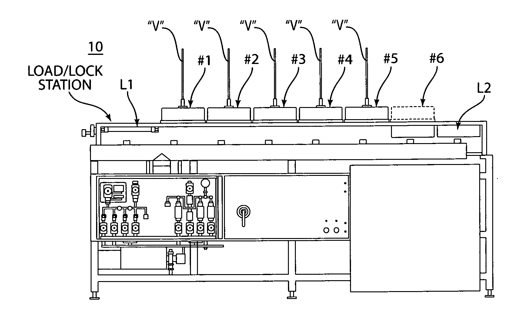
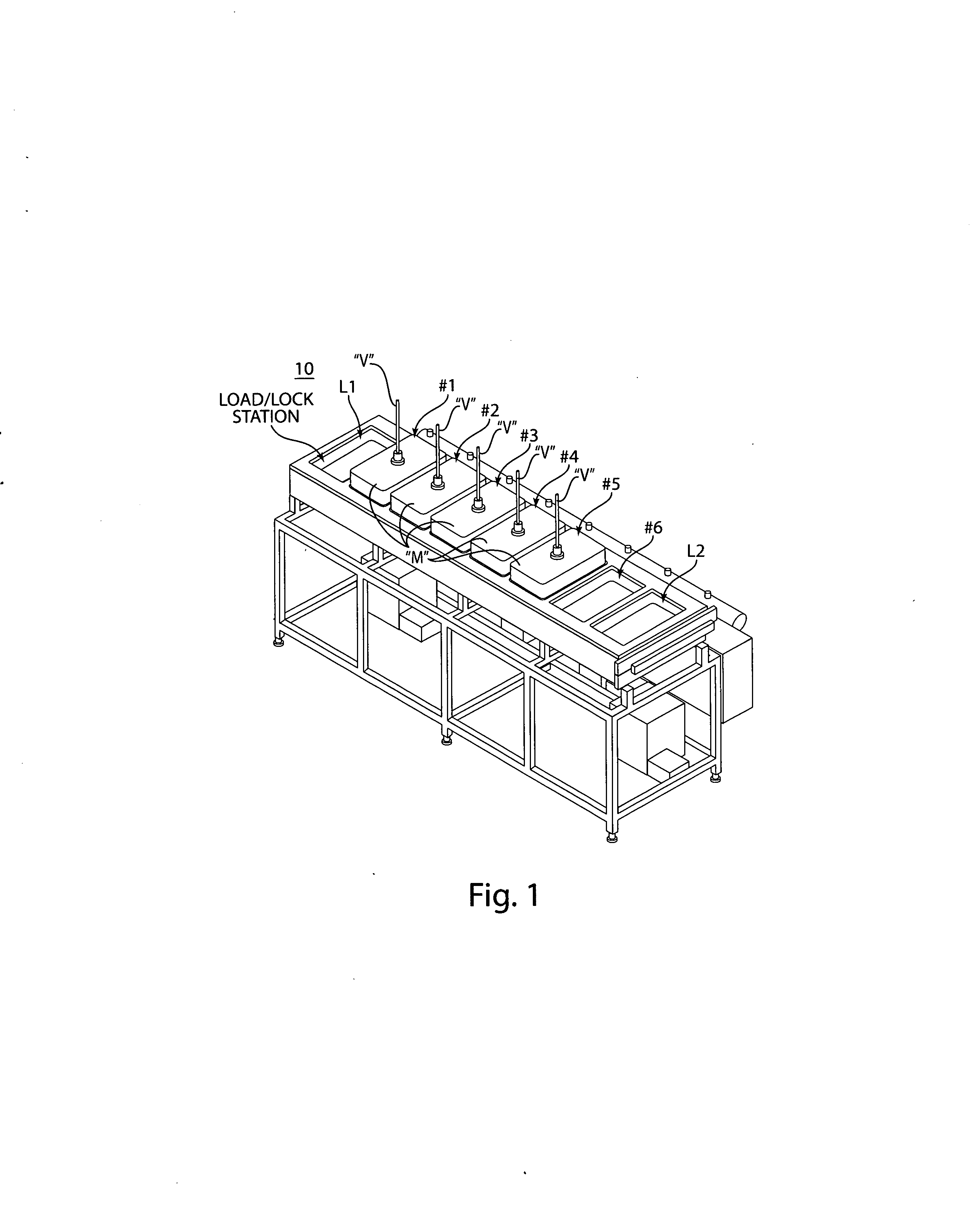
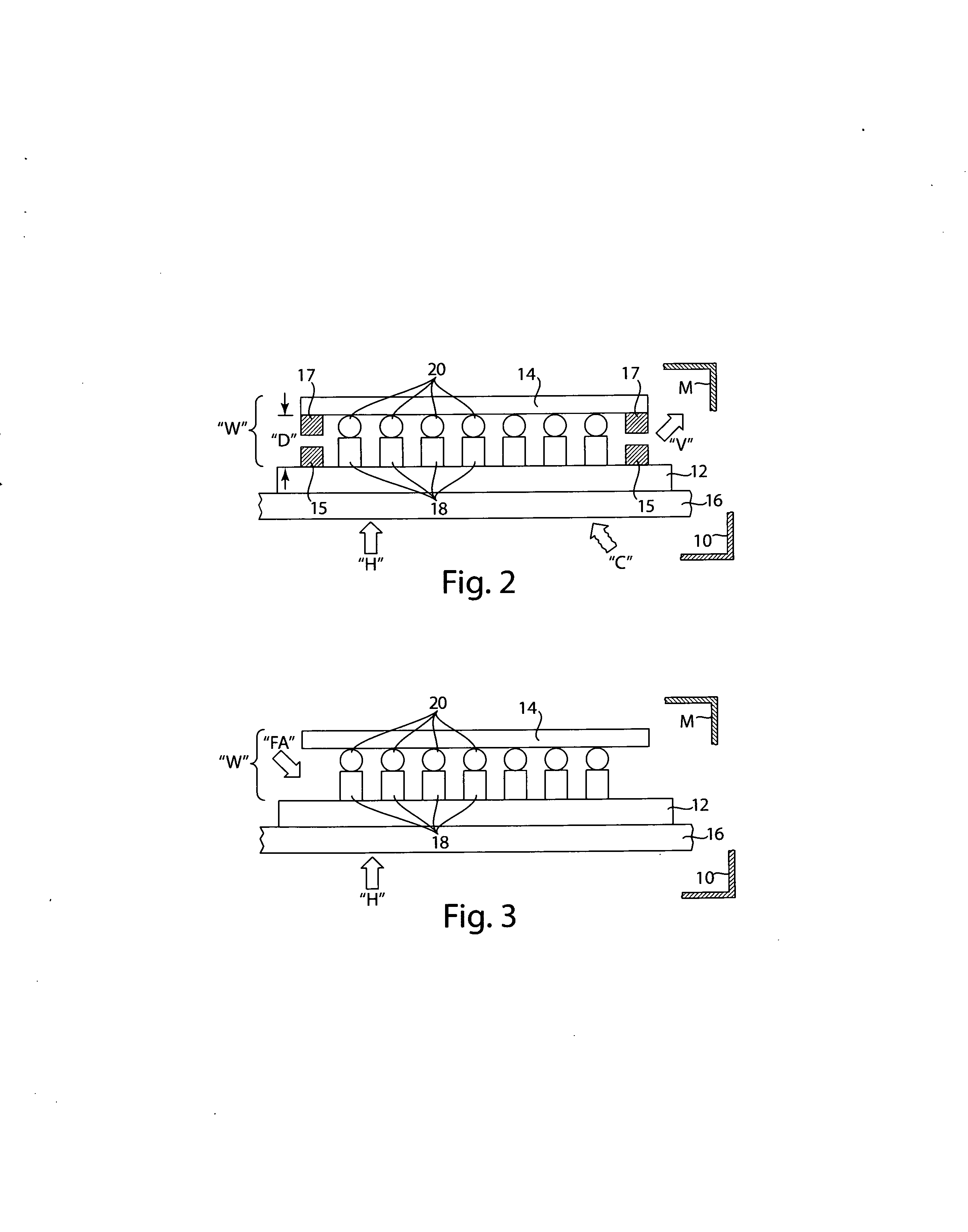
[0048]The invention comprises an electronic chip made by a chip manufacturing process which comprises a stepwise and linearly arranged, serial thermal processing station arrangement 10 using a method for serially treating a pre-assembled chip or die and a substrate assembly “W” through a series of at least six independent, enclosed station chambers and an initial load / lock chamber and a final unload / lock chamber, in the processor arrangement 10, as represented in FIG. 1.

[0049]The linear production station arrangement 10 represented in FIG. 1 is arranged to stepwise present a material to be treated, such as a semiconductor substrate assembly, at a series of linearly aligned, spaced-apart locations, from an initial Load / Lock station to processing stations numbered herein, for example, numbers 1 through 6, which stations each are arranged to independently control the temperature, pressure and atmosphere thereat, as is similarly represented in various aspects and embodiments of the arra...


PUM

PropertyMeasurementUnit
pressureaaaaaaaaaa
temperatureaaaaaaaaaa

Abstract

A linear, serial chip/substrate assembly processing machine for stepwise advancing a pre-assembled chip/die substrate on a support plate through a series of sealable chambers having displacable bottom processing portions. The process begins at a loading station and ends up at an unloading station after various melting and vacuuming of chip/substrate components supported on a device tray through those various chambers to the final joining thereof.

Description

BACKGROUND OF THE INVENTION[0001]1. Field of the Invention[0002]The present invention relates to an electronic chip and to a method of manufacturing same such as semiconductor substrates and more particularly to a stepwise process of a machine utilized in that manufacture of semiconductor substrates and is a continuation-in-part application of co-pending U.S. patent application Ser. No. 12 / 930,462, now U.S. Pat. No. 8,274,161, issuing on 25 Sep. 2012, which is a continuation-in-part application of Ser. No. 12 / 930,203 (Semigear-20) filed 31 Dec. 2010, and wherein the present application claims the benefit of Semigear-20, and also is a CIP of Ser. No. 12 / 653,454; filed Dec. 14, 2009, which is a division of Ser. No. 11 / 482,838, filed Jul. 7, 2006, now U.S. Pat. No. 7,632,750; which is a CIP of Ser. No. 10 / 832,782, filed Apr. 27, 2004, now U.S. Pat. No. 7,008,879, which is a division of Ser. No. 10 / 186,823, filed Jul. 1, 2002, now U.S. Pat. No. 6,827,789; each incorporated herein by ref...

Claims


Application Information

Patent Timeline
Patent Type & Authority Applications(United States)
IPC IPC(8): H01L21/67
CPCB23K1/0016B23K1/008H01L2224/131H01L2224/8109H01L2224/81815H01L2224/81211H01L2224/81205B23K1/206B23K2201/42H01L21/67173H01L24/75H01L24/81H01L2224/81054H01L2224/81065H01L2224/81097H01L2224/81193H01L2924/00014H01L2924/00012H01L2924/014H01L2924/01322B23K2101/42H01L2924/00
Inventor ZHANG, JIANLEE, CHUNGHSIN
Owner SEMLGEAR INC
Why Eureka
Try Eureka