Substrate transfer device and substrate processing system

a technology of substrate and transfer device, which is applied in the direction of coatings, liquid surface applicators, electrical devices, etc., can solve the problems of further degradation of position accuracy, and achieve the effect of suppressing the positional deviation of substra

Inactive Publication Date: 2013-07-18
TOKYO ELECTRON LTD
View PDF0 Cites 395 Cited by
  • Summary
  • Abstract
  • Description
  • Claims
  • Application Information

AI Technical Summary

Benefits of technology

[0017]According to the present invention, since the drive unit is controlled to obtain in advance information on a reference position of the substrate at room temperature when the substrate is loaded into the vacuum processing unit, calculate a positional deviation from the reference position of the substrate when the substrate is loaded into the vacuum processing unit in actual processing, and control the drive unit such that the substrate is loaded into the vacuum processing unit by correcting the positional deviation, in the substrate processing apparatus performing a process accompanied by heat in vacuum, it is possible to suppress the positional deviation of the substrate even if the substrate is transferred at a high speed, correct thermal expansion or the like and increase the positional accuracy of the substrate.

Problems solved by technology

In addition, if a process accompanied by heat such as a film formation process is performed, the positional accuracy may be further degraded by errors due to thermal expansion.

Method used


Image

  • Substrate transfer device and substrate processing system
  • Substrate transfer device and substrate processing system
  • Substrate transfer device and substrate processing system

Examples


Embodiment Construction

[0042]Hereinafter, embodiments of the present invention will be described in detail with reference to the accompanying drawings which forms a part hereof.

[0043](Substrate Processing System of First Embodiment)

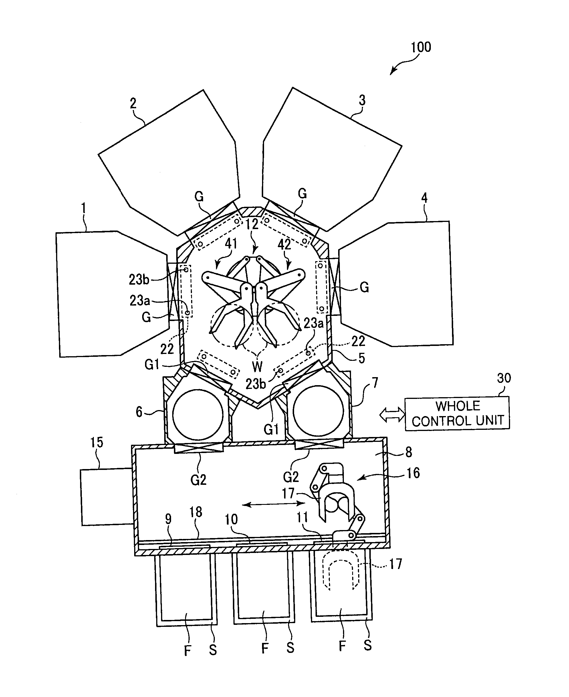
[0044]FIG. 1 is a horizontal cross-sectional view showing a schematic structure of a multi-chamber type substrate processing system in accordance with a first embodiment of the present invention.

[0045]A substrate processing system 100 includes four vacuum processing units 1, 2, 3 and 4 performing a high temperature process, such as a film formation process, accompanied by heat. The vacuum processing units 1 to 4 are respectively provided corresponding to four sides of a hexagonal transfer chamber 5. In addition, load-lock chambers 6 and 7 in accordance with this embodiment are respectively provided at the other two sides of the transfer chamber 5. A loading / unloading chamber 8 is provided at the sides of the load-lock chambers 6 and 7 opposite to the transfer chamber 5. At the ...


PUM


Abstract

A substrate transfer device includes a pick which has positioning pins to position a substrate and holds a positioned substrate; a drive unit which drives the pick such that the substrate is loaded/unloaded to/from a vacuum processing unit by using a pick; and a transfer control unit which controls a transfer operation of the substrate using the pick. The transfer control unit obtains in advance information on a reference position of the substrate at room temperature when the substrate is loaded into the vacuum processing unit, calculates a positional deviation from the reference position of the substrate when the substrate is loaded into the vacuum processing unit in actual processing, and controls a drive unit such that the substrate is loaded into the vacuum processing unit by correcting the positional deviation.

Description

CROSS-REFERENCE TO RELATED APPLICATIONS[0001]This application claims priority to Japanese Patent Application No. 2011-157162 filed on Jul. 15, 2011 and Japanese Patent Application No. 2012-077694 filed on Mar. 29, 2012, the entire contents of which are incorporated herein by reference.FIELD OF THE INVENTION[0002]The present invention relates to, e.g., a substrate transfer device being used in a substrate processing apparatus performing a vacuum process accompanied by heat on a substrate such as a semiconductor wafer, and a substrate processing system.BACKGROUND OF THE INVENTION[0003]In a process of manufacturing a semiconductor device, a vacuum process such as a film formation process is frequently used on a substrate to be processed, i.e., a semiconductor wafer (hereinafter simply referred to as a wafer). In recent years, in terms of improving the efficiency of vacuum processing and suppressing contamination such as oxidation or dust, there has been used a multi-chamber type (clust...

Claims


Application Information

Patent Timeline
Patent Type & Authority Applications(United States)
IPC IPC(8): H01L21/677
CPCH01L21/67739H01L21/68707H01L21/67742
Inventor SAKAUE, HIROMITSUOZAWA, MASAHITOFURUYA, YUICHISHINODA, NANAKOHIROSE, KATSUHITOINAGAKI, MORIHITO
Owner TOKYO ELECTRON LTD
Why Eureka
Try Eureka