Wafer transport apparatus

a technology for transporting apparatuses and wafers, which is applied in the direction of electrical apparatus, conveyor parts, storage devices, etc., can solve the problems of increasing the size of wafers, increasing the cost and technical viewpoint, and contaminating the interior of the wafer transport chamber, so as to improve the wafer transporting capability

Inactive Publication Date: 2013-07-18
SINFONIA TECHNOLOGY CO LTD
View PDF11 Cites 9 Cited by
  • Summary
  • Abstract
  • Description
  • Claims
  • Application Information

AI Technical Summary

Benefits of technology

[0017]According to the present invention, a path in which an unprocessed wafer is carried into a semiconductor manufacturing processing apparatus and a path in which a processed wafer is carried out from the semiconductor manufacturing processing apparatus can be separated from each other. This allows provision of a wafer transport apparatus which is capable of preventing and inhibiting a contaminant deposited on an unprocessed wafer from adhering to a processed wafer or a FOUP to store the processed wafer and has achieved improved wafer-transporting capability.

Problems solved by technology

However, today when the integration degree of elements is increasing, circuits are being miniaturized, and the size of wafers is increasing, management of a speck of dust in the whole clean room is becoming difficult from cost and technical viewpoints.
Additionally, a wafer transport robot sliding in the wafer transport chamber may stir a gaseous atmosphere in the wafer transport chamber, and the interior of the wafer transport chamber may be contaminated with the contaminant.

Method used


Image

  • Wafer transport apparatus
  • Wafer transport apparatus
  • Wafer transport apparatus

Examples


Embodiment Construction

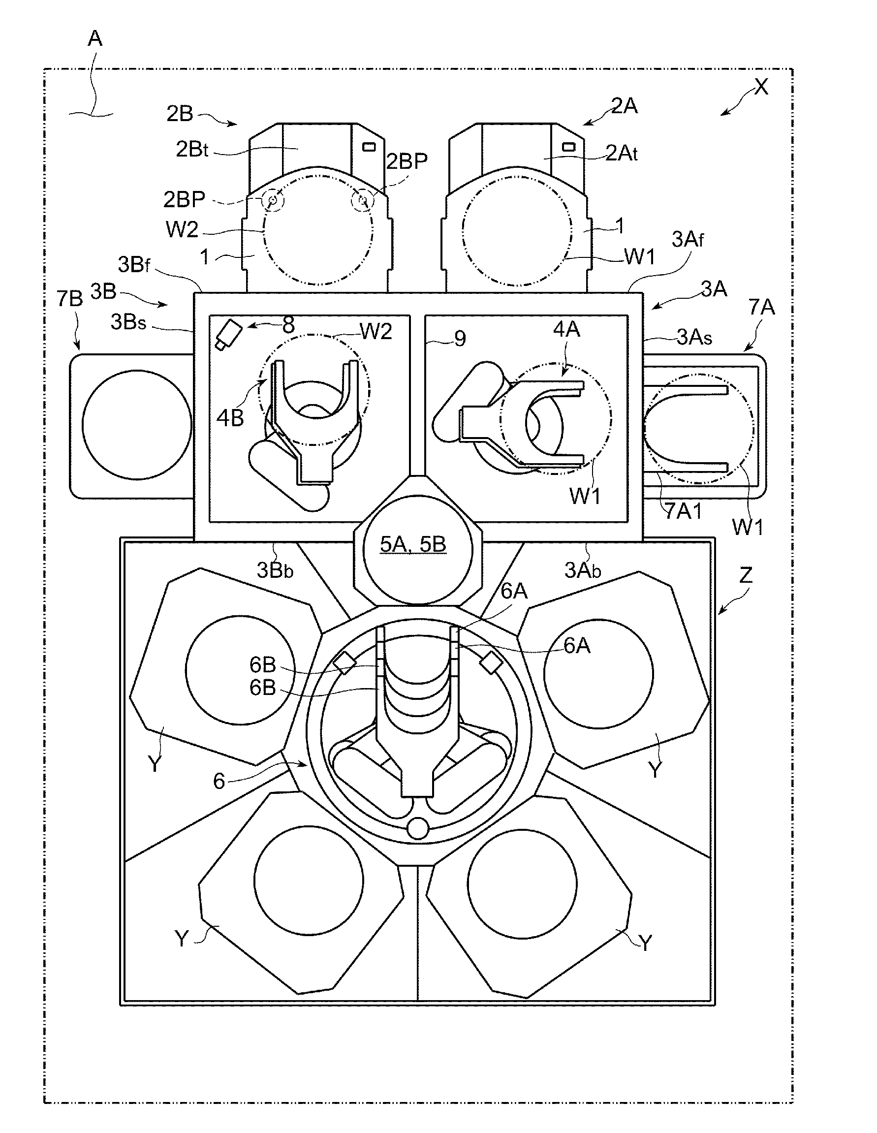
[0023]In the following, an embodiment of the preset invention is described with reference to the accompanying drawing.

[0024]As shown in FIG. 1, a wafer transport apparatus X according to the present embodiment is used, for example, in a semiconductor manufacturing process and is capable of carrying a wafer stored in a FOUP 1 into a semiconductor manufacturing processing apparatus Y (hereinafter also referred to as a “wafer processing apparatus Y”) and carrying out a wafer processed by the wafer processing apparatus Y into the FOUP 1.

[0025]As shown in FIG. 1, the wafer transport apparatus X according to the present embodiment includes a carrying-in load port 2A which can be loaded with the FOUP 1 storing a wafer before processing (hereinafter referred to as an “unprocessed wafer W1”), a carrying-in chamber 3A having a front surface 3Af at which the carrying-in load port 2A is arranged, an in-carrying-in-chamber wafer transport robot 4A which is provided in the carrying-in chamber 3A,...


PUM

PropertyMeasurementUnit
sizeaaaaaaaaaa
processing efficiencyaaaaaaaaaa
adhesionaaaaaaaaaa

Abstract

The wafer transport apparatus prevents contaminant deposited on an unprocessed wafer from adhering to a processed wafer. Carrying-in load port 2A is loaded with a FOUP 1 storing an unprocessed wafer W1. Carrying-in chamber 3A has a transport robot 4A which takes out the unprocessed wafer W1 from the FOUP 1. Carrying-in load lock 5A is accessed by the transport robot 4A from the carrying-in chamber 3A side. Carrying-out load port 2B is loaded with the FOUP 1 that can store a processed wafer W2. Carrying-out chamber 3B has a transport robot 4B which passes the processed wafer W2 to the FOUP 1. Carrying-out load lock 5B is accessed by the transport robot 4B from the carrying-out chamber 3B side. The carrying-in chamber 3A and carrying-out chamber 3B are separated from each other. The carrying-in load lock 5A and carrying-out load lock 5B are arranged on different stages.

Description

BACKGROUND OF THE INVENTION[0001]1. Field of the Invention[0002]The present invention relates to a wafer transport apparatus arranged in a clean room and capable of transporting a wafer.[0003]2. Description of the Related Art[0004]In a semiconductor manufacturing process, wafers are processed in a clean room to improve yield and quality. However, today when the integration degree of elements is increasing, circuits are being miniaturized, and the size of wafers is increasing, management of a speck of dust in the whole clean room is becoming difficult from cost and technical viewpoints. For this reason, means for performing wafer transport and other processing, using a “mini-environment system” that improves the cleanliness of only a local space around a wafer instead of improving the cleanliness of the whole clean room, has recently been adopted. In the mini-environment system, a wafer in a storage container called a FOUP (Front-Opening Unified Pod) for transporting and retaining a ...

Claims


Application Information

Patent Timeline
Patent Type & Authority Applications(United States)
IPC IPC(8): H01L21/677
CPCH01L21/67201H01L21/67739
Inventor MIZOKAWA, TAKUMIKITAZAWA, YASUYOSHI
Owner SINFONIA TECHNOLOGY CO LTD
Why Eureka
Try Eureka