Semiconductor device and method for manufacturing the same

a semiconductor and semiconductor technology, applied in the direction of semiconductor devices, electrical devices, transistors, etc., can solve the problems of difficult to obtain stable semiconductor characteristics, metal film oxidation, hydrogen diffusion, etc., and achieve excellent and stable electric characteristics

Active Publication Date: 2013-07-25
SEMICON ENERGY LAB CO LTD
View PDF13 Cites 57 Cited by
  • Summary
  • Abstract
  • Description
  • Claims
  • Application Information

AI Technical Summary

Benefits of technology

[0032]A self-aligned transistor including an oxide semiconductor film, which has excellent and stable electric characteristics can be provided. Furthe...

Problems solved by technology

However, in this method, hydrogen might diffuse to the channel formation region and it is difficult to obtain stable semiconductor characteristics.
However, in this method, the metal film is oxidized by being subjected to heat treatment in the oxidizing gas atmosphere after formation of the metal film.
If the metal film is not completely oxidize...

Method used


Image

  • Semiconductor device and method for manufacturing the same
  • Semiconductor device and method for manufacturing the same
  • Semiconductor device and method for manufacturing the same

Examples


embodiment 1

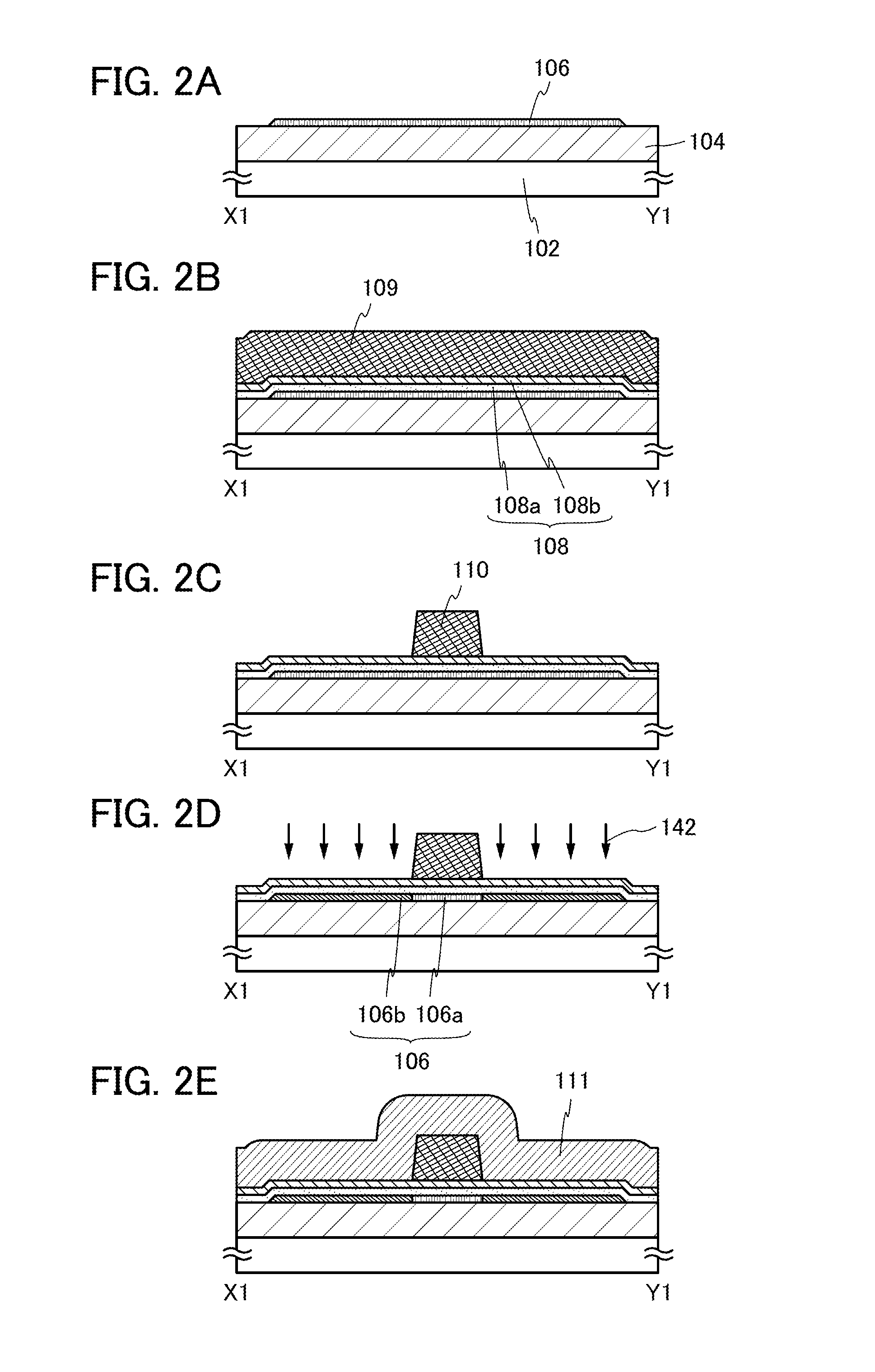
[0066]In this embodiment, an embodiment of a semiconductor device and a method for manufacturing the semiconductor device will be described with reference to FIGS. 1A and 1B, FIGS. 2A to 2E, FIGS. 3A to 3E, and FIGS. 4A to 4D.

example 1

STRUCTURE EXAMPLE 1 OF SEMICONDUCTOR DEVICE

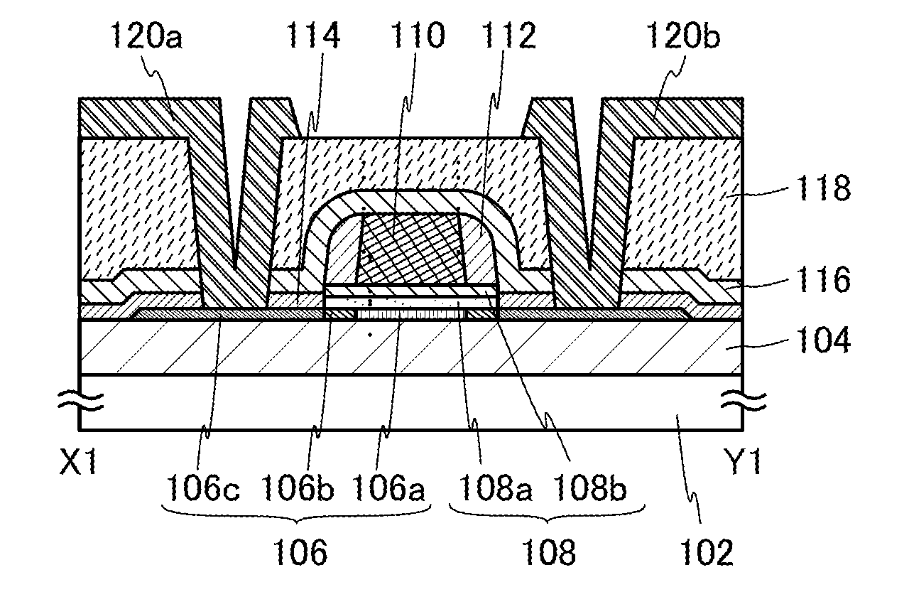
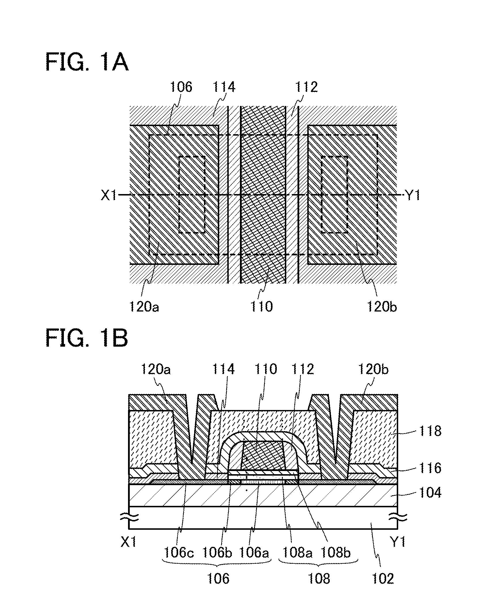
[0067]FIGS. 1A and 1B are a plan view and a cross-sectional view of a top-gate self-aligned transistor as an example of a semiconductor device. FIG 1A is a plan view and FIG. 1B is a cross-sectional view taken along line X1-Y1 in FIG. 1A. Note that in FIG. 1A, some components of the transistor (e.g., a gate insulating film 108) are not illustrated for simplification.

[0068]The semiconductor device illustrated in FIGS. 1A and 1B includes a substrate 102, an oxide film 104 formed over the substrate 102, an oxide semiconductor film 106 which is formed over the oxide film 104 and includes a channel formation region 106a and low-resistance regions 106c having resistance lower than that of the channel formation region 106a, metal oxide insulating films 114 formed in contact with the low-resistance regions 106c, a gate insulating film 108 formed over the oxide semiconductor film 106, a gate electrode 110 which is formed in contact with the gate ins...

embodiment 2

[0179]In this embodiment, a modification example of the semiconductor device described in Embodiment 1, and a method for manufacturing a semiconductor device, which is different from that described in Embodiment 1, will be described with reference to FIGS. 5A and 5B, FIGS. 6A to 6E, FIGS. 7A to 7E, and FIGS. 8A to 8D. Note that portions similar to those in FIGS. 1A and 1B, FIGS. 2A to 2E, FIGS. 3A to 3E, and FIGS. 4A to 4D are denoted by the same reference numerals, and description thereof is skipped.


PUM


Abstract

A metal element of a metal film is introduced into the oxide semiconductor film by performing heat treatment in the state where the oxide semiconductor film is in contact with the metal film, so that a low-resistance region having resistance lower than that of a channel formation region is formed. A region of the metal film, which is in contact with the oxide semiconductor film, becomes a metal oxide insulating film by the heat treatment. After that, an unnecessary metal film is removed. Thus, the metal oxide insulating film can be formed over the low-resistance region.

Description

BACKGROUND OF THE INVENTION[0001]1. Field of the Invention[0002]The present invention relates to a semiconductor device and a method for manufacturing the semiconductor device.[0003]In this specification, a semiconductor device generally means a device which can function by utilizing semiconductor characteristics, and an electrooptic device, a semiconductor circuit, and an electronic appliance are all semiconductor devices.[0004]2. Description of the Related Art[0005]Attention has been focused on a technique for forming a transistor using a semiconductor thin film formed over a substrate having an insulating surface (also referred to as a thin film transistor (TFT)). The transistor is applied to a wide range of electronic devices such as an integrated circuit (IC) or an image display device (display device). A silicon-based semiconductor material is widely known as a material for a semiconductor thin film applicable to a transistor. As another material, an oxide semiconductor has be...

Claims


Application Information

Patent Timeline
IPC IPC(8): H01L29/786H01L29/66
CPCH01L29/78693H01L29/66969H01L29/7869H01L29/78621H01L29/4908H01L27/1225
Inventor YAMAZAKI, SHUNPEISUZUKI, YUKIENODA, KOSEIOIKAWA, YOSHIAKI
Owner SEMICON ENERGY LAB CO LTD
Why Eureka
Try Eureka