System and Method for Thin Film Photovoltaic Modules and Back Contact for Thin Solar Cells

a solar cell and back contact technology, applied in the field of thin film photovoltaic modules and back contact for thin solar cells, can solve the problems of solar cell instability and performance degradation, non-ideal solutions, and unstable formation of stable cells, and achieve the effect of improving cdte photovoltaic devices/modules

Active Publication Date: 2016-01-28
NEW JERSEY INSTITUTE OF TECHNOLOGY
View PDF5 Cites 4 Cited by
  • Summary
  • Abstract
  • Description
  • Claims
  • Application Information

AI Technical Summary

Benefits of technology

[0010]The present disclosure provides advantageous thin film photovoltaic devices/modules and related methods of fabrication. M

Problems solved by technology

However, the formation of a stable, ohmic contact to the active semiconductor has historically presented difficulties.
It is noted that some non-ideal solutions to these problems exist, and such solutions have, to a greater or lesser degree, d

Method used


Image

  • System and Method for Thin Film Photovoltaic Modules and Back Contact for Thin Solar Cells
  • System and Method for Thin Film Photovoltaic Modules and Back Contact for Thin Solar Cells
  • System and Method for Thin Film Photovoltaic Modules and Back Contact for Thin Solar Cells

Examples


example 1

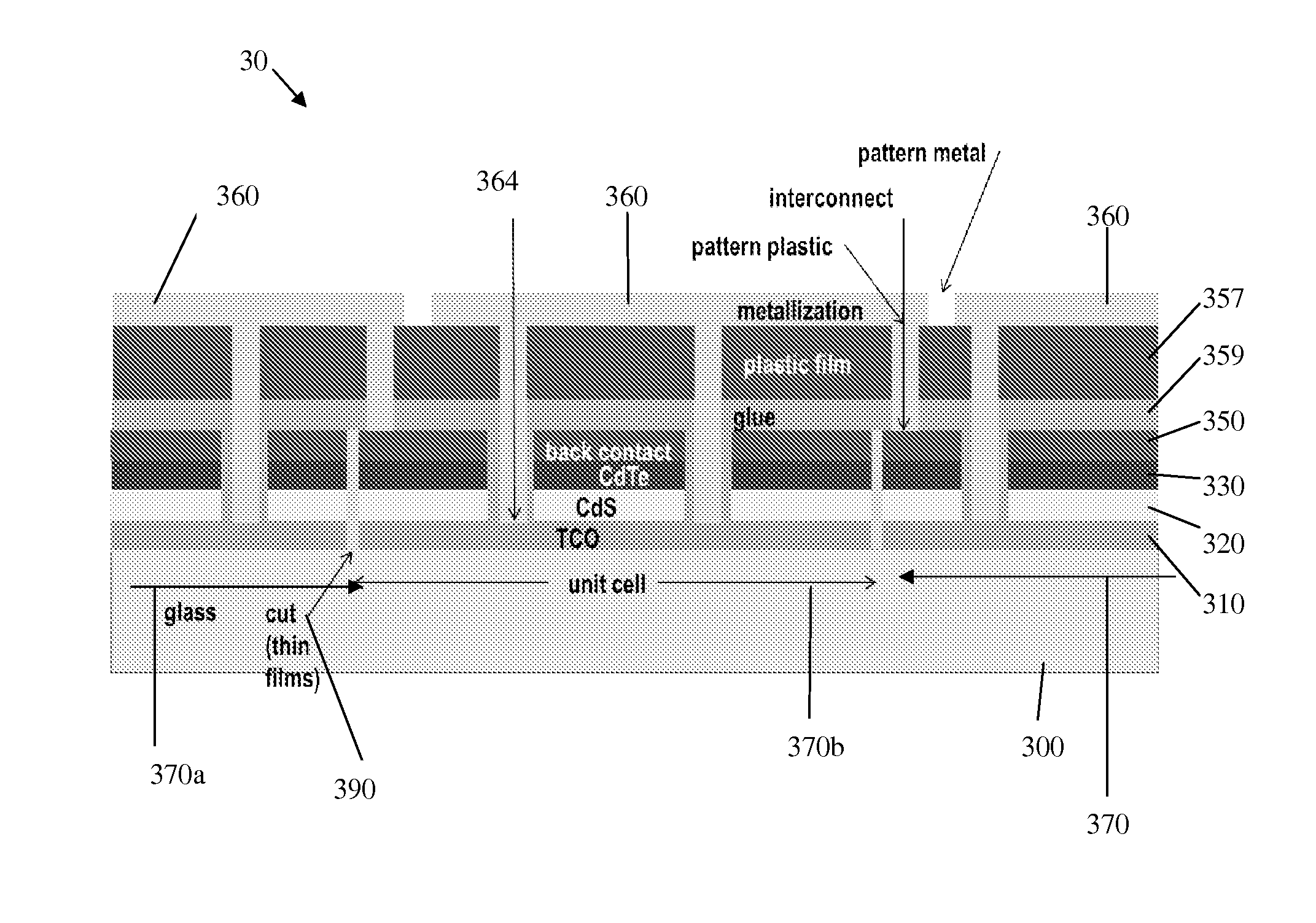
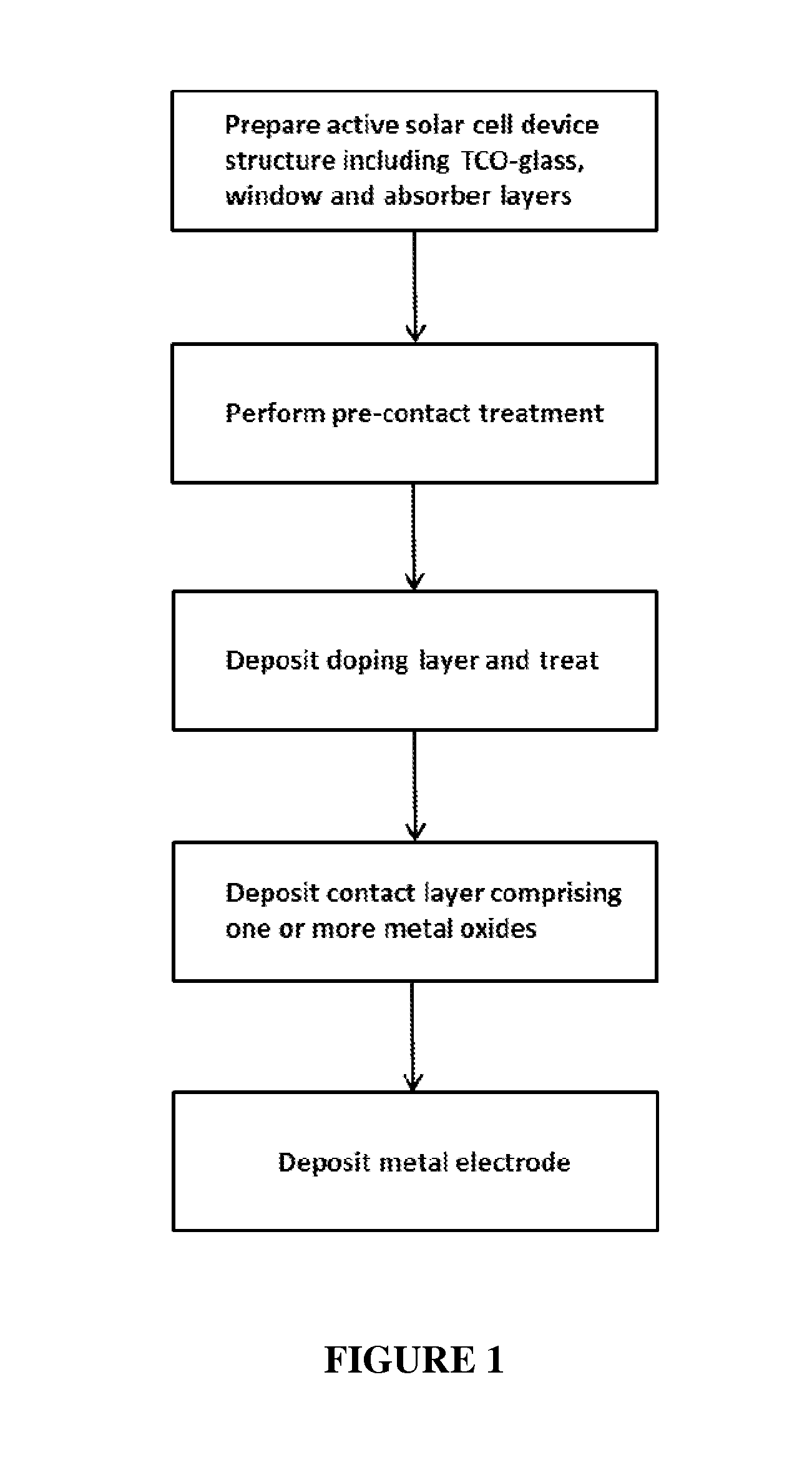
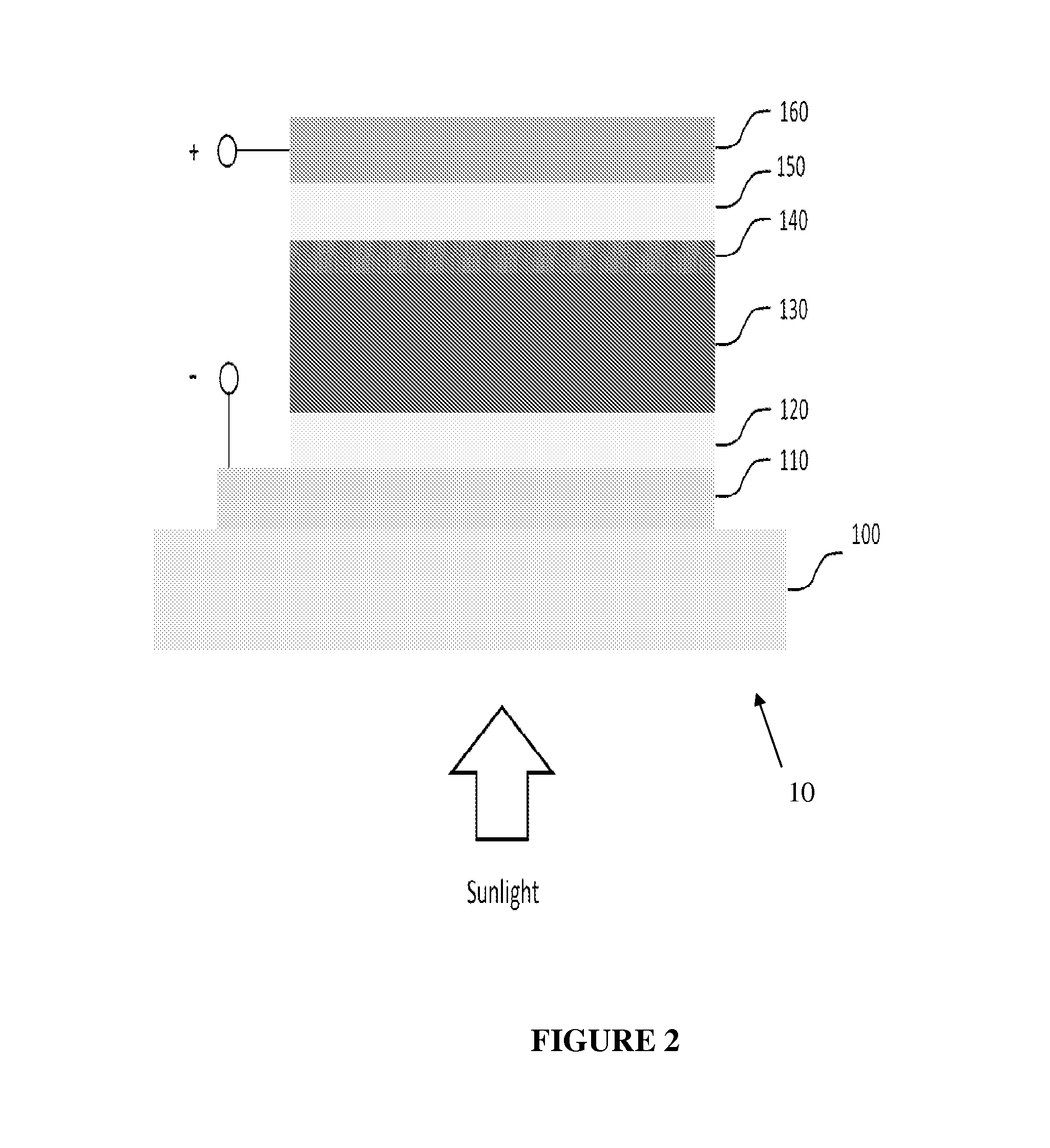
[0053]In exemplary embodiments of the present disclosure and as shown in FIGS. 1-2, the structure of the active solar cell or photovoltaic device 10 is first formed. For example, the transparent substrate 100 (e.g., glass substrate layer 100) can be coated with a transparent conductor (TCO) 110. The transparent conductor layer 110 can include a transparent conducting oxide overcoated with a high resistive layer, or of other similar such layer performing such function.

[0054]A window layer 120 is then positioned on the transparent conductor layer 110. In exemplary embodiments, the window layer 120 can include CdS or oxygenated CdS, and can be deposited by chemical bath deposition, sputtering, or other suitable means / processes.

[0055]A semiconductor absorber layer 130 is then positioned on the window layer 120. In certain embodiments, the semiconductor absorber layer 130 includes CdTe, and can be deposited by close-spaced sublimation, vapor transport deposition or other suitable means / p...

example 2

[0077]In general, experience has been accumulated in the past few years regarding the installation of large photovoltaic power stations. It has been realized that, when the module voltage is relatively high, e.g. about 90V, then for the common 600 V DC maximum input voltage to the inverter, the number of modules in each series string is typically limited to about 6. This increases the number of strings and the associated quantity of materials required in terms of cables, protecting diodes, and other materials / facilities, thereby increasing the balance-of-system (BOS) cost associated with the power station. If the module voltage is a little under 60V, then about 10 modules can generally be connected in a single string. As such, a trend is towards lower module voltages. For example, the Sharp 235 W monocrystalline silicon module has an even lower open-circuit voltage (Voc) of about 37 V (with a short circuit current or Isc of about 8.5 A), thereby allowing about 15 modules in a single...


PUM


Abstract

The present disclosure provides improved thin film photovoltaic devices and related methods of fabrication. More particularly, the present disclosure provides improved CdTe photovoltaic devices and related fabrication methods. Disclosed is a novel thin film photovoltaic device and means for its fabrication. An exemplary device includes a metal oxide layer between the absorber layer and the rear electrode, resulting in an ohmic back contact and having improved device stability. The metal oxide layer can include at least one of silver oxide or copper oxide, and may additionally contain nickel oxide, molybdenum oxide, and/or vanadium oxide. The present disclosure is directed towards formation of a ohmic back contact for solar cells, the back contact having improved stability. In certain embodiments, the present disclosure provides for an ohmic contact to p-type II-VI semiconductors, and to the fabrication of solar cells having improved stability, and to solar panels incorporating such back contact schemes.

Description

CROSS-REFERENCE TO RELATED APPLICATIONS[0001]This application claims the benefit of: (i) U.S. Provisional Application Ser. No. 61 / 777,735 filed Mar. 12, 2013, and (ii) U.S. Provisional Application Ser. No. 61 / 777,784 filed Mar. 12, 2013, the contents of each being herein incorporated by reference in their entireties.FIELD OF THE DISCLOSURE[0002]The present disclosure relates to improved thin film photovoltaic devices or modules and related methods of fabrication and, more particularly, to improved CdTe photovoltaic devices or modules and related methods of fabrication.BACKGROUND OF THE DISCLOSURE[0003]In general, solar cells and photovoltaic modules based on II-VI semiconductors (e.g., CdTe) are known and exist as commercial products. However, the formation of a stable, ohmic contact to the active semiconductor has historically presented difficulties. It is noted that some non-ideal solutions to these problems exist, and such solutions have, to a greater or lesser degree, drawbacks ...

Claims


Application Information

Patent Timeline
IPC IPC(8): H01L31/18H01L31/0224H01L31/0296
CPCH01L31/1884H01L31/0296H01L31/022466H01L31/02245H01L31/18Y02E10/50
Inventor CHENG, ZIMENGCHIN, KEN K.DELAHOY, ALAN E.
Owner NEW JERSEY INSTITUTE OF TECHNOLOGY
Why Eureka
Try Eureka