

Capping Layers for Improved Crystallization
a technology of crystallization and capping layers, applied in the direction of superimposed coating process, natural mineral layered products, transportation and packaging, etc., can solve the problems of high cost, high cost, high cost, etc., and achieve the effect of improving photovoltaic devices
- Summary
- Abstract
- Description
- Claims
- Application Information
AI Technical Summary
Benefits of technology
Problems solved by technology
Method used
Image

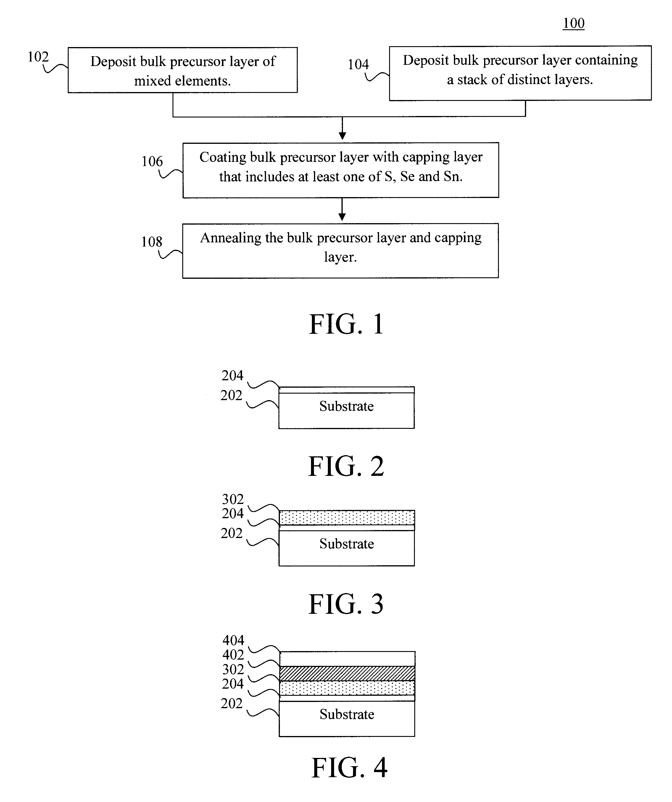
Examples
example 1
[0052]A bulk layer was prepared according to the method described in U.S. Patent Application Publication No. 2011 / 0094557:
[0053]All operations were performed in a nitrogen-filled glove box. A solution for depositing the bulk precursor layer was prepared in two parts in glass vials under magnetic stirring: A1, by dissolving Cu2S, 0.573 grams (g) and sulfur, 0.232 g in 3 milliliters (ml) of hydrazine and B1, by mixing SnSe, 0.790 g, Se, 1.736 g and Zn, 0.32 g with 7 ml of hydrazine. After 3 days under magnetic stirring, solution A1 had an orange transparent aspect, while solution B1 was dark green and opaque. Solutions A1 and B1 were mixed (to form solution C1) before deposition.
[0054]A solution (D1) for depositing a Sn-containing capping layer was prepared by dissolving 0.12 g SnS and 0.88 g Se in 4 ml of hydrazine.
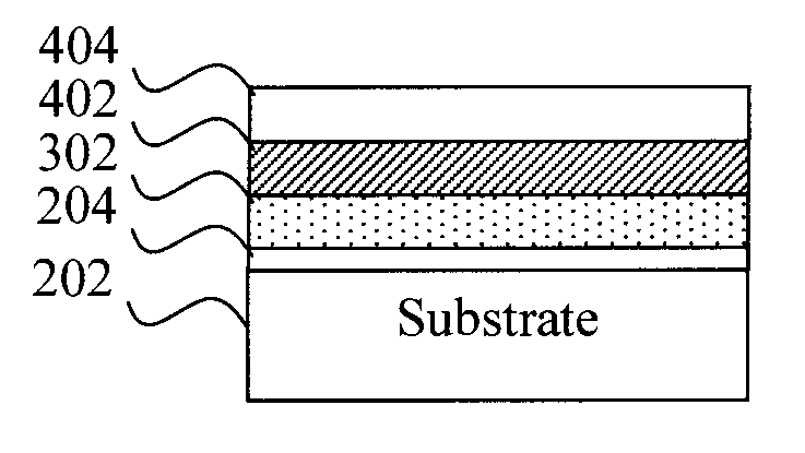
[0055]A bulk precursor film was deposited on a soda lime glass substrate coated with 700 nm molybdenum by spin coating at 800 revolutions per minute (rpm) and heating the ...
example 2
[0057]A bulk layer was prepared the same as in example 1 except for employing less selenium (1.405 g) in the solution B2, mixed with solution A1 to form solution C2. Capping solution E2 contained only selenium (0.880 g) in 4 ml of hydrazine.
[0058]Films were then prepared as described in conjunction with the description of Example 1, above: Sample P was prepared by spin coating 5 layers of solution B2. Sample Q was prepared by spin coating 5 layers of solution B2 and a layer of solution E2, containing only selenium. Sample R was prepared by spin coating 5 layers of solution B2 and a layer of solution D1, containing selenium and tin.
example 3
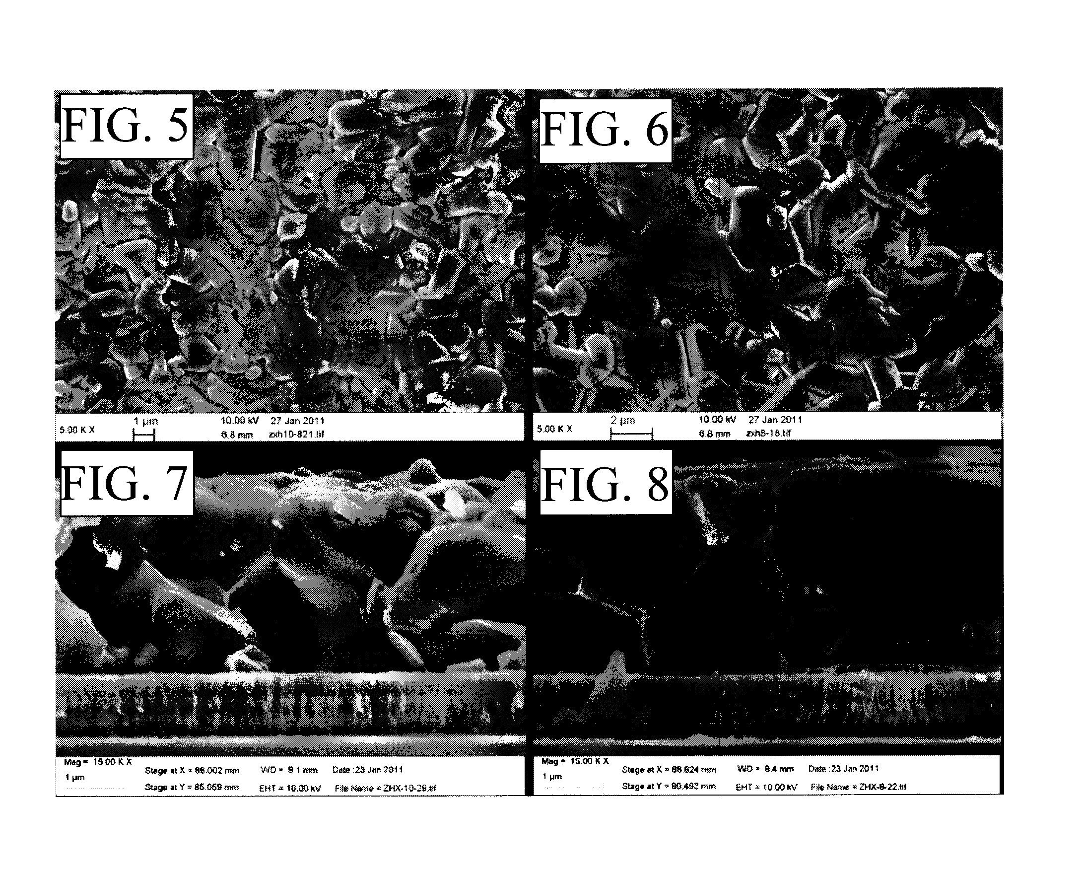
[0059]Solar cells with approximate area of 0.45 square centimeters (cm2) were fabricated from the obtained kesterite films sample P type and sample R type by deposition of 60 nm CdS buffer layer by chemical bath deposition, 100 nm insulating ZnO and 130 nm ITO (indium-doped zinc oxide) by sputtering. Statistically significant efficiency enhancement of 19% average was found when samples were treated with a capping layer. See FIG. 9. FIG. 9 is an efficiency distribution of all samples of type P prepared with no capping layer and all samples of type R prepared with SnS—Se capping layer.
[0060]A discussion of the example results now follows. FIGS. 5 and 7 present surface and cross-section SEM images, respectively, of films without a capping layer, which show grain size in the range of from about 1 micrometer to about 2 micrometers. FIGS. 6 and 8 present surface and cross-section SEM images, respectively, of identically processed films with SnS—Se capping layer D1 which show larger grain ...
PUM
| Property | Measurement | Unit |
|---|---|---|
| thickness | aaaaa | aaaaa |
| thickness | aaaaa | aaaaa |
| temperature | aaaaa | aaaaa |
Abstract
Description
Claims
Application Information