Solar Cell Structure

a solar cell and structure technology, applied in the field of photovoltaic structure, can solve the problems of insufficient to meet the needs of most applications, the conversion efficiency of organic solar cells is typically significantly lower, and the cost of most applications is too high, so as to improve the conversion efficiency and enhance the photoelectric conversion efficiency

Inactive Publication Date: 2011-07-14
KOCHERGIN VLADIMIR
View PDF3 Cites 6 Cited by
  • Summary
  • Abstract
  • Description
  • Claims
  • Application Information

AI Technical Summary

Benefits of technology

[0027]It is an object of the present invention to provide an improved photovoltaic device utilizing plasmon resonance-based enhancement of the photoelectric conversion efficiency which will resolve the majority of deficiencies of prior art approaches and will provide external quantum efficiency of organic photovoltaic devices compatible to that of thin film silicon photovoltaic devices or, if applied to nonorganic photovoltaic devices, will significantly improve the conversion efficiency beyond what is available with state of the art devices. It is another object of the present invention to provide a method of manufacturing of the photovoltaic device of the present invention.

Problems solved by technology

The common problem of these devices (except the multijunction solar cells, which are too expensive for most applications) is the need to utilize optically “thick” photovoltaic absorbers (or active layers, which are typically semiconductors) to enable efficient light absorption and photocarrier current collection.
High efficiency cells must have minority carrier diffusion lengths exceeding the active layer thickness by several times. This represents serious problem and tradeoff for a number of commonly used solar cell materials, most prominent for organic solar cells.
However, roll-to-roll conversion efficiencies for organic solar cells are typically significantly lower than the record numbers (as with any other technology) and are still insufficient to meet the needs of most applications.
First, the limited absorption range of current materials leads to inefficient photon harvesting.
The low charge carrier mobility in organic materials limits the possible active layer thickness.
However, the effect on total (angular and spectrally-integrated) quantum efficiency was not reported and most probably was quite small.
The main disadvantage of this invention is generally narrow band of conversion efficiency enhancement in such an apparatus due to spectrally narrow (resonant) phase matching conditions between photons and surface plasmon, leading to very small if any overall improvement of the photovoltaic device performance.
The disadvantage of this apparatus is spectrally and angularly narrow band of enhancement of photoelectric conversion efficiency.
The main disadvantage of the referenced photovoltaic device is generally narrow spectral range of surface Plasmon enhancement of the photoresponse, poorly overlapping with solar spectrum.
The disadvantage of such a device is still the too narrow spectral and / or angular band of enhanced photovoltaic conversion.
The disadvantage of all the disclosed so far plasmonic photovoltaic structures is the limited (spectrally and / or angularly) band of conversion efficiency enhancement, which in turn limits the overall plasmonic improvement of the solar energy generation.
Unfortunately, the widening of the plasmonic band in such nanostructures is typically accompanied with significant red-shifting of the band from visible to near IR wavelengths (for gold or silver composites) accompanied by the reduction of the absorption in the blue portion of the spectrum, reducing the potential utility of such an approach for solar cells.

Method used


Image

  • Solar Cell Structure
  • Solar Cell Structure
  • Solar Cell Structure

Examples


first embodiment

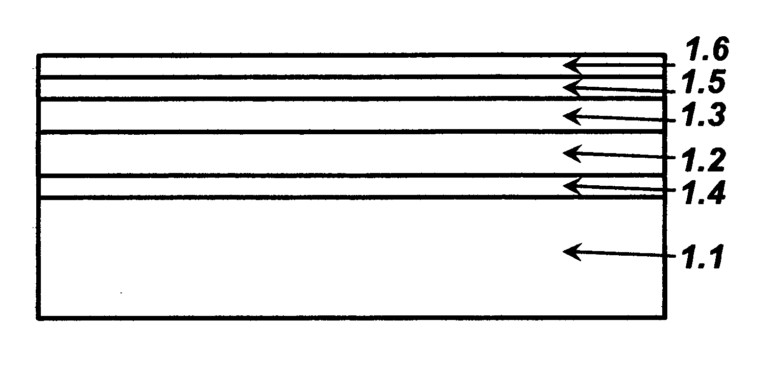
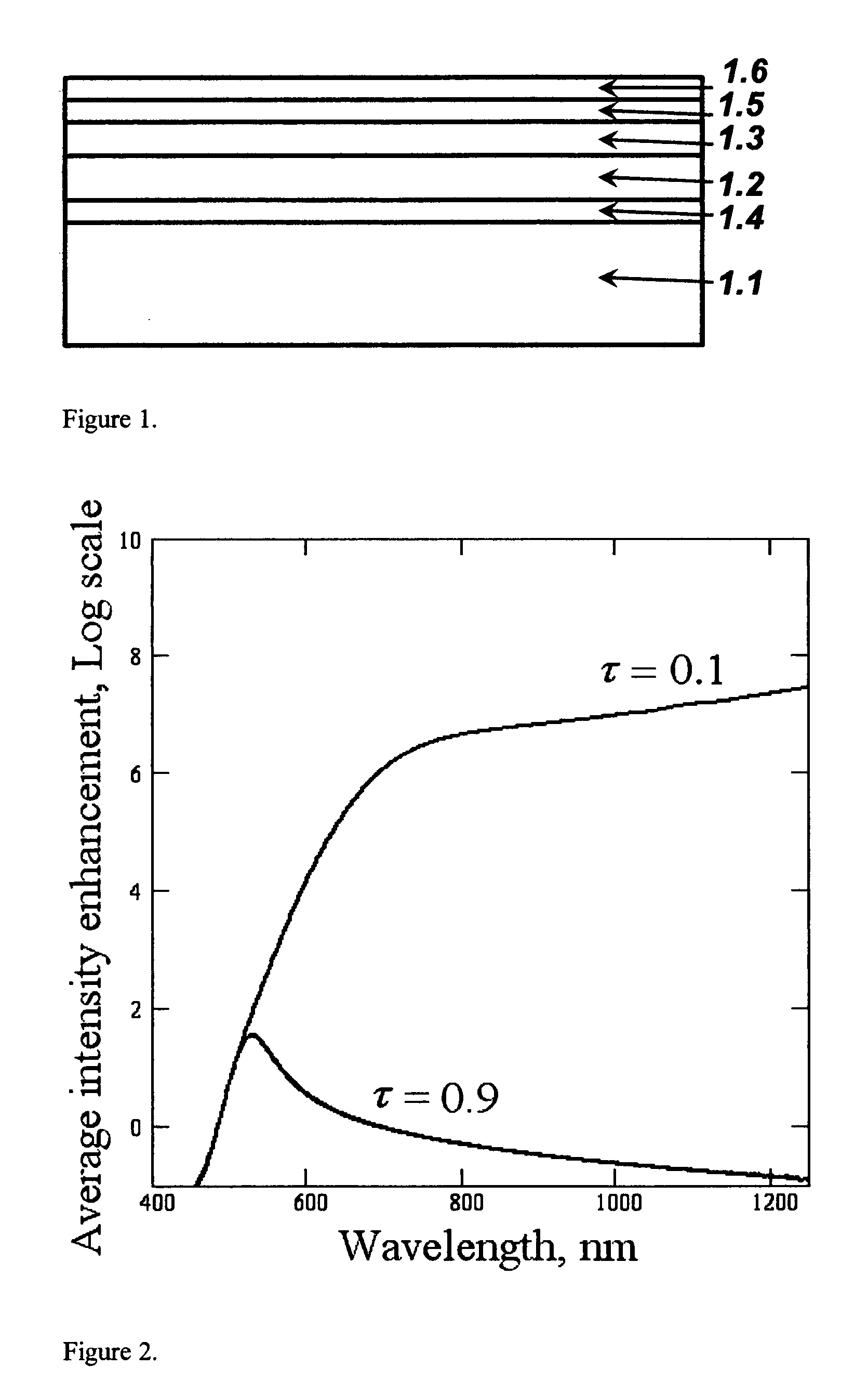
[0054]According to the present invention the Plasmon-enhanced photovoltaic device shown in FIG. 1 is comprising a substrate 1.1; at least one photoconversion layer 1.2 disposed on said substrate, a plasmonic nanostructure layer 1.3 disposed on the surface of photoconversion layer, said plasmonic nanostructure layer having concentration of metal close to percolation threshold. and at least two electrodes 1.4 and 1.5, a first of which electrodes is in electrical contact with a first charge collection region of photoconversion layer in which electrical charges of a first polarity are concentrated, and a second of which electrodes is in electrical contact with a second charge collection region of said photoconversion layer in which electrical charges of a second polarity are concentrated. Additional protection and / or antireflection layer 1.6 can be employed in photovoltaic device as well to further improve the performance.

[0055]The photoconversion layer can be made of polycrystalline, s...

second embodiment

[0069]According to the present invention the Plasmon-enhanced photovoltaic device shown in FIG. 6 is comprising a substrate 6.1, a plasmonic nanostructure layer 6.3 disposed on said substrate, said plasmonic nanostructure layer having concentration of metal close to percolation threshold, at least one photoconversion layer 6.2 disposed on said plasmonic nanostructure layer, and at least two electrodes 6.4 and 6.5, a first of which electrodes is in electrical contact with a first charge collection region of photoconversion layer in which electrical charges of a first polarity are concentrated, and a second of which electrodes is in electrical contact with a second charge collection region of said photoconversion layer in which electrical charges of a second polarity are concentrated. Additional protection and / or antireflection layer 6.6 can be employed in photovoltaic device as well to further improve the performance.

[0070]All aspects disclosed in relation to the first embodiment are...

third embodiment

[0072]According to the present invention the method of manufacturing of a Plasmon-enhanced photovoltaic device comprises, as illustrated in FIG. 7: providing a substrate 7.1, applying, onto said substrate, first electrode 7.4, applying, onto said first electrode, a plasmonic nanostructure layer made of metal 7.2, said plasmonic nanostructure layer having concentration of metal close to percolation threshold, applying a photoconversion layer onto said plasmonic nanostructure layer, 7.3 and applying, onto said photoconversion layer a second electrode 7.5. Optionally, the second electrode can be coated with antireflection and / or protection layer 7.6.

[0073]Deposition of the first electrode (Step 1 in FIG. 7) and second electrode (Step 4 in FIG. 7) can be performed by physical vapor deposition (magnetron sputtering, Ion Assisted Ion Beam Deposition, Thermal Evaporation), chemical vapor deposition (including but not limited to metal-organic chemical vapor deposition, low pressure chemical...


PUM


Abstract

Utilization of the near percolation plasmonic nanostructures near the photoconversion layer in photovoltaic device provide significant enhancement in the efficiency. Photovoltaic devices utilizing efficiency enhancement due to utilization of near percolation plasmonic nanostructures and methods of photovoltaic device fabrication provide an improved solar cells that can be used for power generation and other applications.

Description

CROSS-REFERENCES TO RELATED APPLICATIONS[0001]Not applicable.STATEMENT REGARDING FEDERALLY SPONSORED RESEARCH OR DEVELOPMENT[0002]Not applicable.FIELD OF THE INVENTION[0003]The present invention is related to a photovoltaic structure. In more detail, the present invention is related to the plasmon-enhanced photovoltaic structure utilizing plasmon-enhanced absorption and improved conversion efficiency. The apparatus of the present invention can be applied to solar energy generation used for utilities and other applications.BACKGROUND OF THE INVENTION[0004]A large number of different solar cell and photovoltaic structures are known to those skilled in the art. This includes crystalline silicon, amorphous silicon, multijunction, and organic photovoltaic devices to name a few. The common problem of these devices (except the multijunction solar cells, which are too expensive for most applications) is the need to utilize optically “thick” photovoltaic absorbers (or active layers, which ar...

Claims


Application Information

Patent Timeline
Patent Type & Authority Applications(United States)
IPC IPC(8): H01L31/0256H01L31/04H01L31/0368H01L31/036H01L31/0272H01L31/0296H01L31/0304H01L31/18
CPCH01L31/02168H01L31/022425Y02E10/50H01L31/06H01L31/0232H01L31/054Y02E10/52H01L31/02327
Inventor KOCHERGIN, VLADIMIR
Owner KOCHERGIN VLADIMIR
Why Eureka
Try Eureka