Method for reducing contact resistance of a semiconductor device

a technology of contact resistance and semiconductor, which is applied in the direction of semiconductor devices, basic electric elements, electrical appliances, etc., can solve the problems of increasing contact resistance, unable to effectively reduce contact resistance, and extremely low contact resistance between silicons, so as to improve device operation capability, reduce contact resistance, and improve refresh characteristics

Inactive Publication Date: 2006-04-11
SK HYNIX INC
View PDF12 Cites 2 Cited by
  • Summary
  • Abstract
  • Description
  • Claims
  • Application Information

AI Technical Summary

Benefits of technology

[0017]It is an object of the present invention to provide a method for fabricating a semiconductor device wherein the lower portion of a contact hole formed by etching a buffer layer and a interlayer insulating film is cleaned, ion-imp

Problems solved by technology

That is, the contact resistance between the silicons is extremely low when they have nearly equal impurity concentrations.
Generally, even though a polysilicon layer is deposited after a wet cleaning process without any delays in a conventional contact formation process, the contact resistance cannot be effectively reduced.
As described above, in accordance with the conventional method for f

Method used


Image

  • Method for reducing contact resistance of a semiconductor device
  • Method for reducing contact resistance of a semiconductor device
  • Method for reducing contact resistance of a semiconductor device

Examples


Embodiment Construction

[0021]A method for fabricating a semiconductor device in accordance with a preferred embodiment of the present invention will now be described in detail with reference to the accompanying drawings.

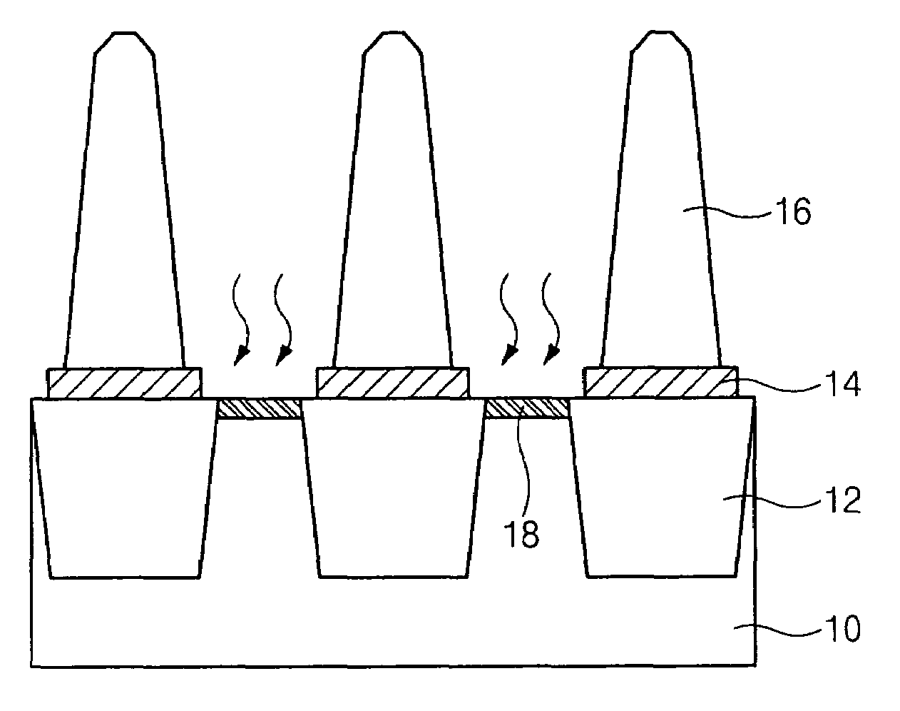
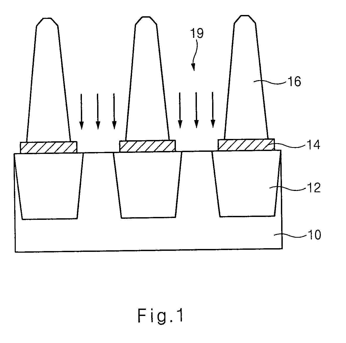
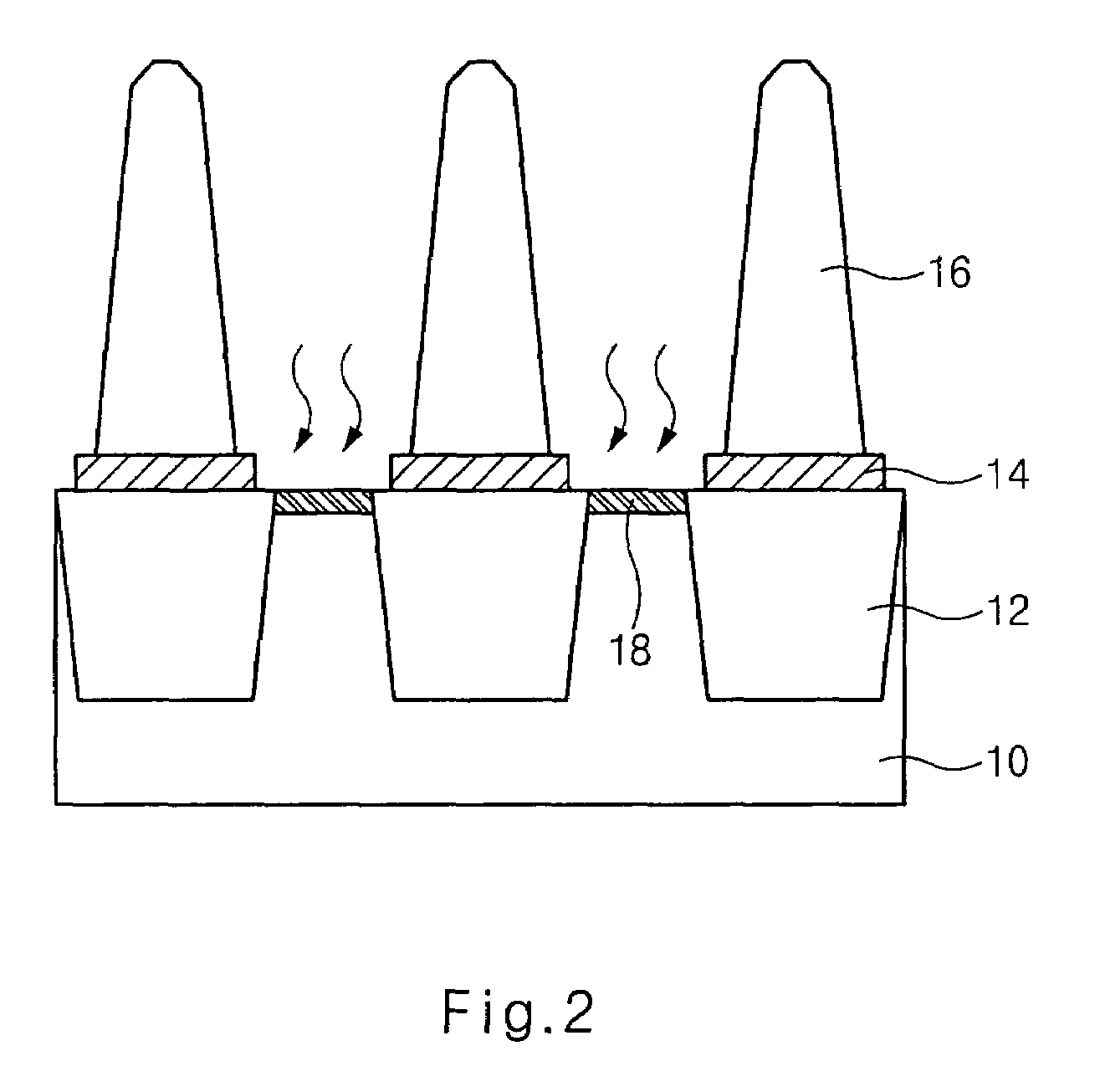
[0022]FIGS. 1 through 3 are cross-sectional diagrams illustrating sequential steps of the method for fabricating the semiconductor device in accordance with the present invention.

[0023]Referring to FIG. 1, a device isolation film 12 defining an active region is formed on a semiconductor substrate 10. The device isolation film 12 is preferably of a trench-type.

[0024]A buffer layer (not shown) having a predetermined thickness is formed on the entire surface of the resulting structure. Preferably, the buffer layer consists of a nitride film, and serves as an etch barrier in a subsequent etching process for forming a contact hole to prevent damages of the active region.

[0025]An interlayer insulating film (not shown) is formed on the buffer layer. Preferably, the interlayer insulating film is a...


PUM


Abstract

A method for fabricating a semiconductor device wherein the lower portion of a contact hole is cleaned, and doped with an impurity for reducing contact resistance is disclosed. The method comprises: sequentially forming a buffer layer and an interlayer insulating film on a semiconductor substrate; etching the interlayer insulating film and the buffer layer to form a contact hole exposing the semiconductor substrate; performing a cleaning process of a lower portion of the contact hole; doping an impurity into the surface of the semiconductor substrate exposed by the contact hole; and forming a conductive layer filling the contact hole on the entire surface of the resulting structure.

Description

BACKGROUND OF THE INVENTION[0001]1. Field of the Invention[0002]The present invention relates to a method for fabricating a semiconductor device, and more particularly to a method for fabricating a semiconductor device wherein the lower portion of a contact hole is cleaned, and doped with an impurity for improving the refresh characteristics and reducing the contact resistance to improve operation capability of the device.[0003]2. Description of the Background Art[0004]As the integration density of semiconductor device is increased, the line width of the device has decreased. A various processes have been developed and used to fabricate devices with excellent characteristics.[0005]In particular, a contact formation process for reducing contact resistances has been newly suggested to improve operation efficiency of a device.[0006]In a conventional semiconductor device, a silicon contact material consists of polysilicon containing impurities. In case of an ideal contact interface, a c...

Claims


Application Information

Patent Timeline
IPC IPC(8): H01L21/302H01L21/28H01L21/311H01L21/768
CPCH01L21/02063H01L21/76814H01L21/31116H01L21/28
Inventor SHIN, DONG SUK
Owner SK HYNIX INC
Why Eureka
Try Eureka