Method of forming an oxinitride layer

a technology of oxynitride and oxide layer, which is applied in the direction of basic electric elements, semiconductor/solid-state device manufacturing, electric apparatus, etc., can solve the problems of poor uniformity and quality of batch-type apparatus, thin oxide or oxynitride layer formed in single-type apparatus may have poor electrical characteristics, etc., to improve the reliability of semiconductor devices, improve the efficiency of forming process, and improve the effect of oxynitride layer throughpu

Inactive Publication Date: 2008-04-17
SAMSUNG ELECTRONICS CO LTD
View PDF10 Cites 2 Cited by
  • Summary
  • Abstract
  • Description
  • Claims
  • Application Information

AI Technical Summary

Benefits of technology

[0034] In one embodiment, the secondarily oxidized substrate is tertiarily oxidized in the first reaction chamber when the first reaction chamber is at the second temperature and the second pressure. According to the present invention, the oxide layer is formed on the substrate using a batch type apparatus, and the oxynitride layer is formed on the substrate using the RTN apparatus. Thus, the throughput of the process for forming the oxynitride layer can be increased and the oxynitride la...

Problems solved by technology

In a conventional semiconductor manufacturing method, the very thin oxide or oxynitride layer is formed using a single type apparatus such as a rapid thermal processing (RTP) apparatus since the very thin oxide or oxynitride layer may not have a precisely controlled thickness and...

Method used


Image

  • Method of forming an oxinitride layer
  • Method of forming an oxinitride layer
  • Method of forming an oxinitride layer

Examples


Embodiment Construction

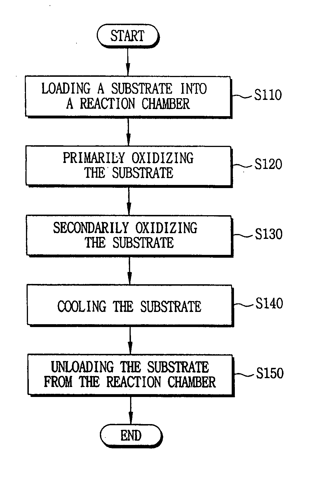
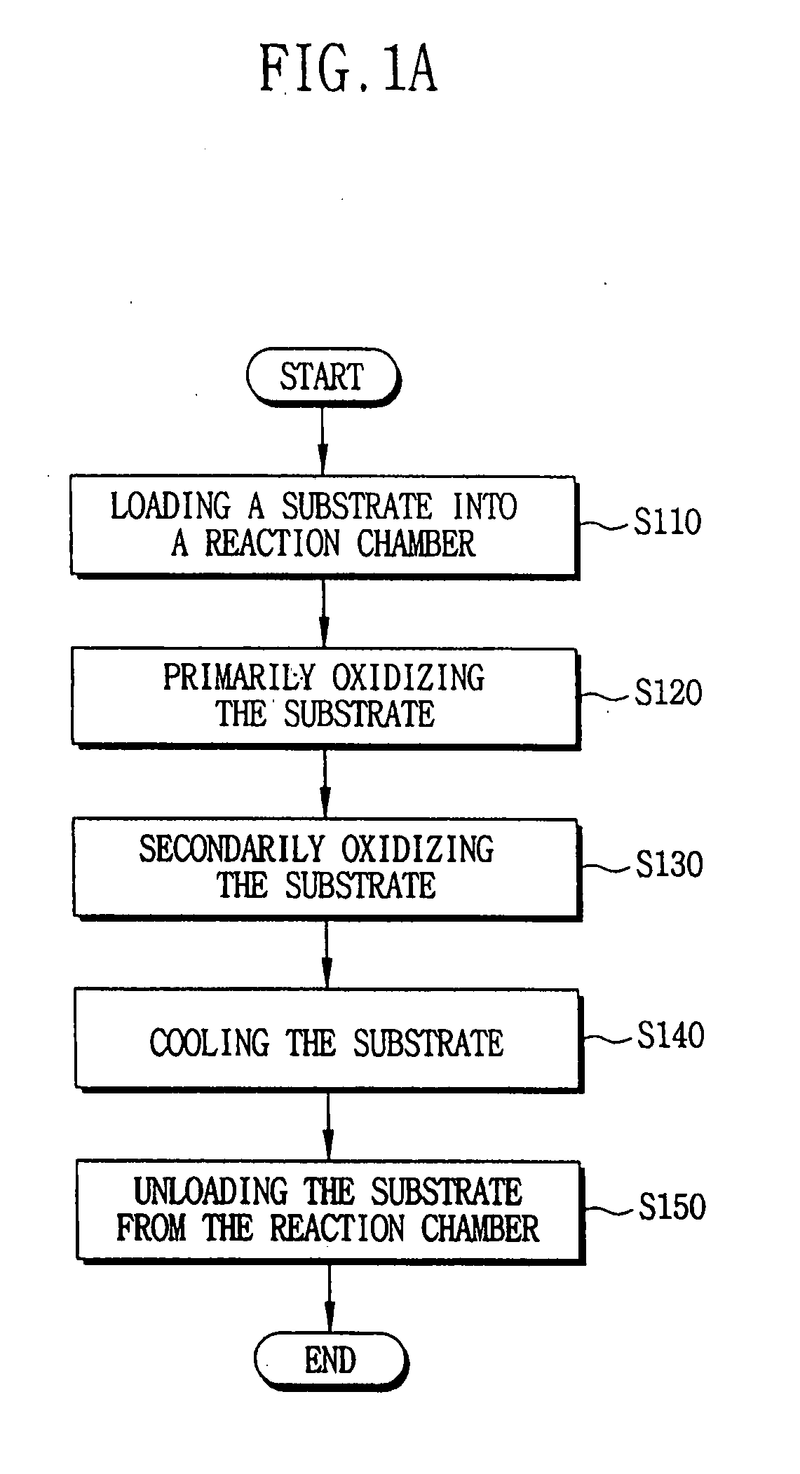
[0054] In the following detailed description, it will be understood that when an element such as a layer, region or substrate is referred to as being “on” or “onto” another element, it can be directly on the other element or intervening elements may also be present.

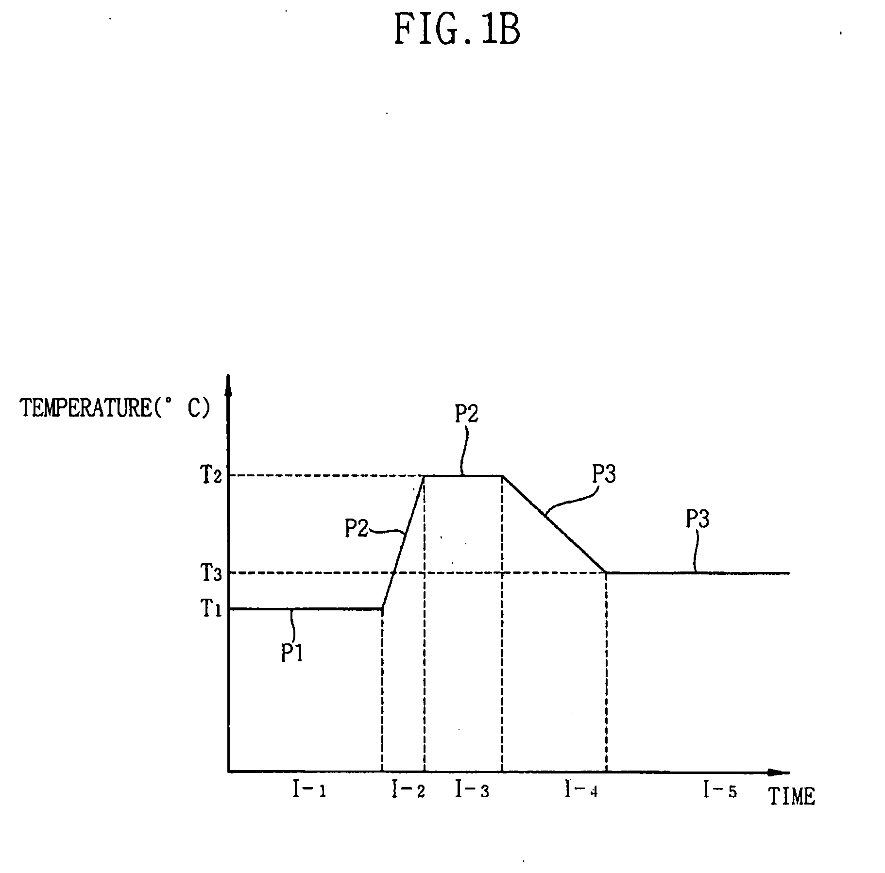
[0055] U.S. Patent Application Publication number 2002-3258 discloses a method of forming a gate insulation layer including a silicon oxynitride layer that is converted from a hydroxy-silicate layer by a nitration process after forming the hydroxy-silicate layer on a substrate. In this approach, the nitration process is carried out at a temperature of about 200 to about 500° C. and a pressure of about 1 to about 5 Torr to form the silicon oxynitride layer having a thickness of about 7 Å. However, since the nitration process is performed in a single type apparatus such as a rapid thermal nitration (RTN) apparatus, the throughput of the nitration process may be reduced and the characteristics of the silicon oxynitride laye...


PUM


Abstract

In methods of forming an oxide layer and an oxynitride layer, a substrate is loaded into a reaction chamber having a first pressure and a first temperature. The oxide layer is formed on the substrate using a reaction gas while increasing a temperature of the reaction chamber from the first temperature to a second temperature under a second pressure. Additionally, the oxide layer is nitrified in the reaction chamber to form the oxynitride layer on the substrate. When the oxide layer and/or the oxynitride layer are formed on the substrate, minute patterns of a semiconductor device, for example a DRAM device, an SRAM device or an LOGIC device may be easily formed on the oxide layer or the oxynitride layer.

Description

CROSS REFERENCE TO RELATED APPLICATION [0001] This application is a divisional of U.S. application Ser. No. 10 / 839,934, filed on May 6, 2004, which claims priority under 35 USC § 119 to Korean Patent Application No. 2003-29446, filed on May 9, 2003, the contents of which are herein incorporated by reference in their entirety for all purposes.BACKGROUND OF THE INVENTION [0002] 1. Field of the Invention [0003] The present invention relates to a method of forming an oxide layer and a method of forming an oxynitride layer. More particularly, the present invention relates to a method of forming a very thin oxide layer having excellent uniformity and characteristics on a substrate using a batch type apparatus, and a method of forming a very thin oxynitride layer by nitrifying the oxide layer on the substrate. [0004] 2. Description of the Related Art [0005] As information processing systems such as computers have been widely utilized, semiconductor devices also have been rapidly developed....

Claims


Application Information

Patent Timeline
IPC IPC(8): H01L21/469H01L21/316H01L21/31
CPCH01L21/0223H01L21/02255H01L21/31662H01L21/0234H01L21/02332H01L21/31
Inventor YOU, YOUNG-SUBLEAM, HUN-HYEOUNGNAM, SEOK-WOOKIM, BONG-HYUNLEE, WOONGLEE, SANG-HOON
Owner SAMSUNG ELECTRONICS CO LTD
Why Eureka
Try Eureka