Inspection apparatus

a technology of inspection apparatus and probe substrate, which is applied in the direction of measurement devices, semiconductor/solid-state device testing/measurement, instruments, etc., can solve the problems of increasing the design cost of the probe substrate, complicated wires from the tester lands on the upper surface of the probe substrate to the respective probes provided on the lower surface, etc., to achieve simplified connection wiring in the probe substrate, reduce mutual noise, and facilitate the effect of equal length wires

Inactive Publication Date: 2013-07-25
NIHON MICRONICS
View PDF3 Cites 5 Cited by
  • Summary
  • Abstract
  • Description
  • Claims
  • Application Information

AI Technical Summary

Benefits of technology

[0008]In the semiconductor inspection apparatus configured as above, connecting the electrical connecting portions on the tester side directly to the probe substrate of the probe card can simplify the configuration of the inspection apparatus and reduce cost of the members. The apparatus can also reduce effects of mutual noises among the wires due to shortening of the wire length from the tester to the probe substrate, which enables a higher frequency inspection.
[0010]The present invention is accomplished by taking such problems as mentioned above into consideration thereof, and an object thereof is to provide an inspection apparatus in which, in an inspection apparatus of a semiconductor wafer, connection between a tester and a probe card is configured with reference to positions of respective chips of the semiconductor wafer to simplify connection wiring in a probe substrate, facilitate wires of equal length, and reduce mutual noises among wires by shortening of the wire length, and to reduce design cost of the probe substrate.
[0012]With the above configuration, in an inspection apparatus for use in an electrical test of a device formed on a semiconductor wafer, connection wiring in a probe substrate can be simplified, wires of equal length are facilitated, mutual noises among wires are reduced by shortening of the wire length, and design cost of the probe substrate can be low.

Problems solved by technology

However, in the above semiconductor inspection apparatus, since arrangement of signal, power, and ground wires connected from the tester circuit to the respective devices is determined with reference to the tester side as in a conventional case, internal wires from the tester lands on the upper surface of the probe substrate to the respective probes provided on the lower surface remain complicated.
Accordingly, it is not easy for the respective wires in the probe substrate to be equal in length, which causes increase in design cost of the probe substrate.

Method used


Image

  • Inspection apparatus
  • Inspection apparatus
  • Inspection apparatus

Examples


Embodiment Construction

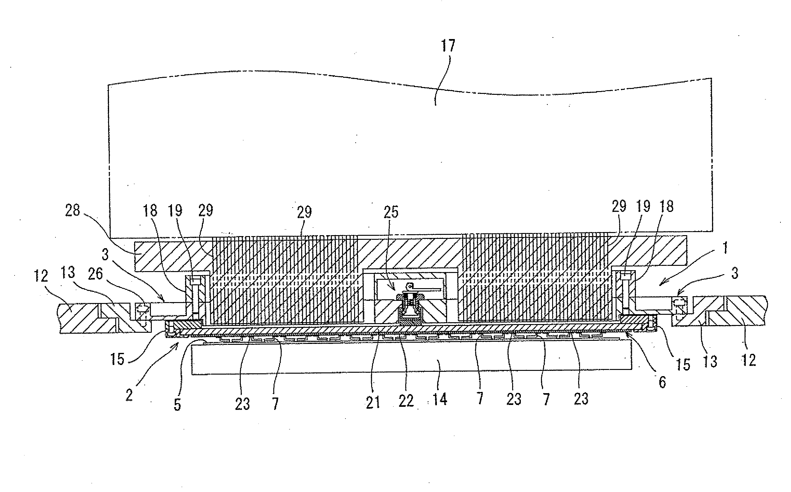
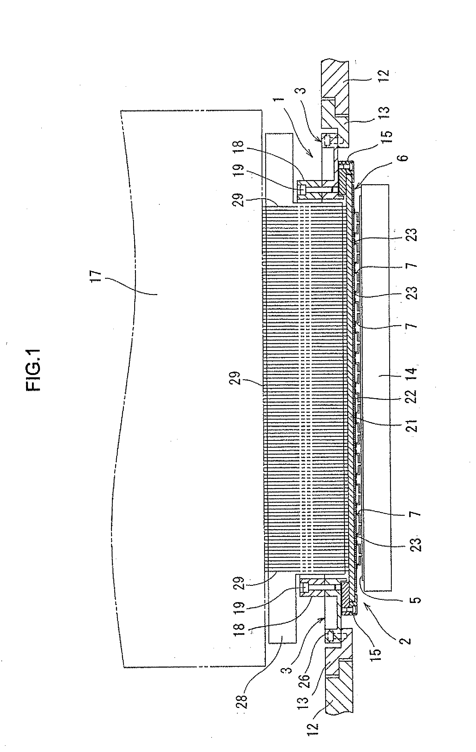
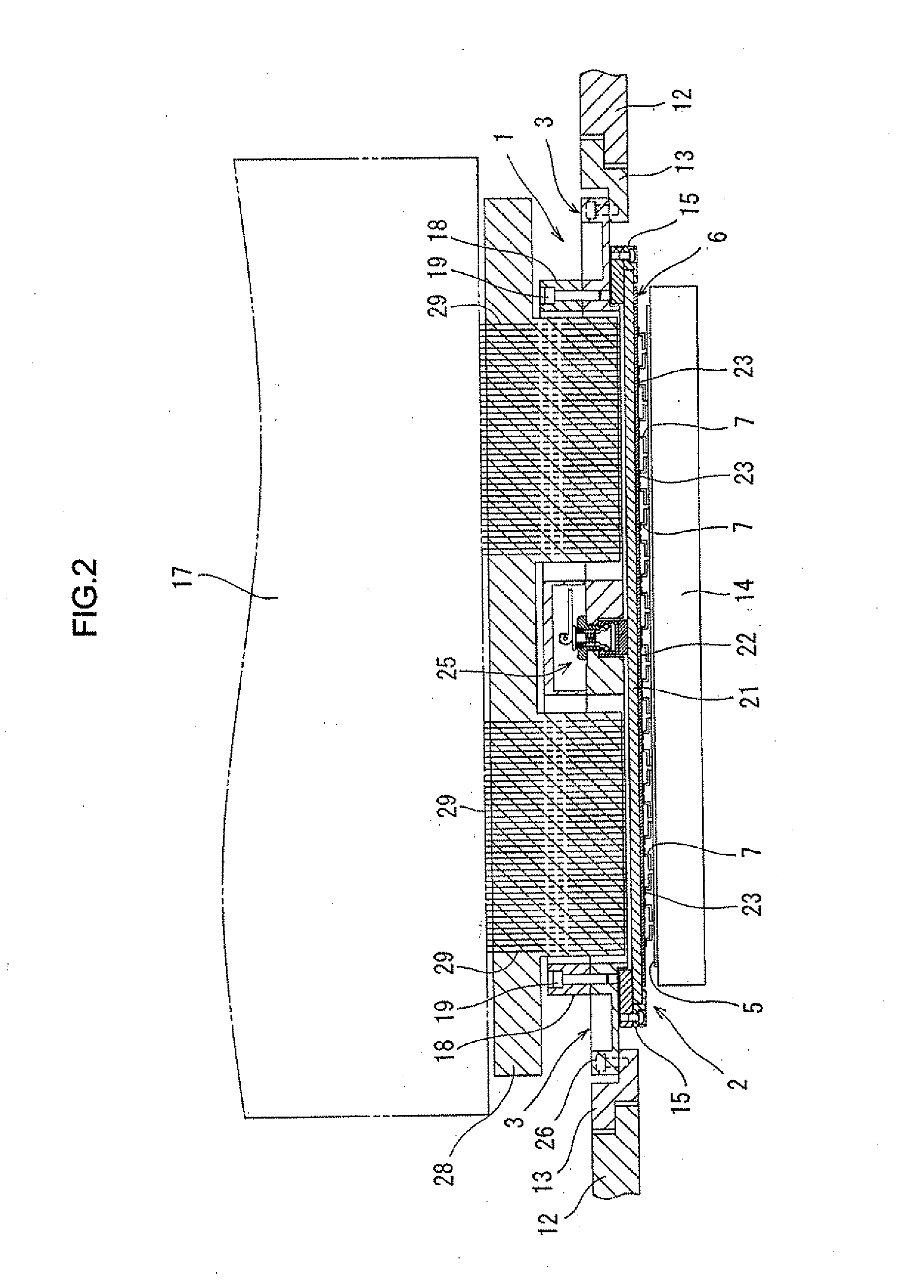
[0020]Hereinafter, an inspection apparatus according to embodiments of the present invention will be described with reference to the attached drawings.

[0021]An inspection apparatus according to the present invention is configured to include a prober mechanism having an XYZθ stage and the like supporting a semiconductor wafer as a plate under inspection, a tester adapted to perform an electrical test of the semiconductor wafer supported on the prober mechanism, and a probe assembly having a probe card adapted to apply test signals on the tester side via a tester head of the tester to respective electrodes of a plurality of chips formed on the semiconductor wafer. As such an inspection apparatus according to the present invention, every existing inspection apparatus having the above probe card can be used. That is, since the inspection apparatus according to the present invention is characterized by an electrical connecting structure between the tester and the probe card, the present ...


PUM


Abstract

An inspection apparatus includes a probe card having a plurality of probes arranged to correspond to each chip of a semiconductor wafer under inspection and contacting a plurality of electrodes of each chip and a test head electrically connected to the respective probes of the probe card and applying test signals from a tester, and a plurality of tester lands of a probe substrate electrically connected respectively to the plurality of probes. A plurality of electrical connecting portions on the tester side of the test head, corresponding to the respective tester lands, are arranged to constitute a plurality of arrangement areas sectioned to correspond to the respective chips under inspection, and the plurality of probes of the probe substrate are connected to the corresponding tester lands provided in the arrangement areas in units of chips under inspection.

Description

CROSS-REFERENCE TO RELATED APPLICATION[0001]This application claims, under 35 USC 119, priority of Japanese Application No. 2012-010294 filed on Jan. 20, 2012.BACKGROUND OF THE INVENTION[0002]1. Technical Field Relating to the Invention[0003]The present invention relates to an inspection apparatus in which electrical connection between a tester and a probe card for use in an electrical test of a device formed on a semiconductor wafer has been improved.[0004]2. Description of Related Art[0005]Electrical connection between a tester and a probe card of an inspection apparatus for use in an electrical test of a device formed on a semiconductor wafer is performed by tester connecting portions provided at the circumference of the probe card as described in Patent Document 1 (Japanese patent Laid-Open No. 2005-17121), for example. That is the tester connecting portions provided at the circumference of the probe card are electrically connected to the tester side, and inspection signals from...

Claims


Application Information

Patent Timeline
Patent Type & Authority Applications(United States)
IPC IPC(8): G01R31/26
CPCG01R31/2889G01R31/26H01L22/00
Inventor WASHIO, KENICHIHASEGAWA, MASASHI
Owner NIHON MICRONICS
Why Eureka
Try Eureka