
Controller, System, and Method for Mapping Logical Sector Addresses to Physical Addresses

a controller and physical address technology, applied in the field of memory devices, can solve the problems of not being able to access random addresses, devices cannot be used for running code directly from flash memory, and not being able to fully match the behavior of sbc and mbc devices

Inactive Publication Date: 2013-07-25
LASSER MENAHEM
View PDF8 Cites 13 Cited by
  • Summary
  • Abstract
  • Description
  • Claims
  • Application Information

AI Technical Summary

Benefits of technology

The present invention provides a controller for a flash memory device that includes a host-type NAND interface for exchanging data pages with the flash memory device and a flash-type NAND interface for exchanging data sectors with the host. The data sectors have a common data sector size that is different than the common physical page size of the pages of the memory. The technical effect of this invention is to allow for efficient data storage and retrieval between the host and the flash memory device, even if the host and the flash memory device have different data page sizes.

Problems solved by technology

It is not possible to access any random address in the way described above for NOR—instead the host has to write into the device a sequence of bytes which identifies both the type of the requested command (e.g. read, write, erase, etc.) and the address to be used for that command.
Because of the non-random access nature of NAND devices, such devices cannot be used for running code directly from their flash memories.
The SBC and MBC devices are not fully identical in their behavior—the time it takes to write an MBC page is much longer than time it takes to write an SBC page.
Typically, NAND devices are relatively difficult to interface and work with.
Another difficulty is the existence of errors in the data read from NAND devices, in contrast to NOR devices that can be assumed to always return correct data.
This inherent non-reliability of NAND devices requires the use of Error Detection Codes (EDC) and Error Correction Codes (ECC).
However, such an architecture suffers from many disadvantages.
First, the host has to individually manipulate each one of the NAND device's control signals (e.g. CLE or ALE), which is cumbersome and time-consuming for the host.
Second, the support of EDC and ECC puts a severe burden on the host—parity bits have to be calculated for each page written, and error detection calculations (and sometimes also error correction calculations) must be performed by the host.
All this makes such “no controller” architecture relatively slow and inefficient.
Flash devices have certain limitations that make using these devices at the physical address level a bit of a problem.
In a flash device, it is not practical to rewrite a previously written area of the memory without a prior erase of the area, i.e. flash cells must be erased (e.g. programmed to “one”) before the cells can be programmed again.
Furthermore, some of the blocks of the device are “bad blocks” that are not reliable, so that the use of these blocks should be avoided.
The latter term is a misnomer, as the implementations do not necessarily support “files”, in the sense that files are used in operating systems or personal computers, but rather support block device interfaces similar to those exported by hard disk software drivers.
There is one further issue of potential complexity in interfacing with NAND-based flash memory devices that must be addressed.
However, when using NAND devices with 2 Kbytespages (or other page sizes that are larger than a sector's size), multiple sectors are assigned to a common flash page, and this creates some complexities, as will be explained below.
If the page is larger than a sector, the burden of mapping and matching data sectors to pages falls on the host.
However, this is not the case—all prior art devices that have a NAND interface that is a logical interface use pages and not sectors as their basic unit of data transfer.
This process is highly inefficient and, as stated above, eliminates the main advantage of having a logical interface in the first place—accessing the memory device according to a simple access model without the host having to be bothered by physical implementation details of the flash memory, such as page size.

Method used


Image

  • Controller, System, and Method for Mapping Logical Sector Addresses to Physical Addresses
  • Controller, System, and Method for Mapping Logical Sector Addresses to Physical Addresses
  • Controller, System, and Method for Mapping Logical Sector Addresses to Physical Addresses

Examples


Embodiment Construction

[0069]The principles and operation of access to a memory device via a NAND interface according to the present invention may be better understood with reference to the drawings and the accompanying description.

[0070]The present invention will now be described in terms of specific exemplary embodiments. It is to be understood that the invention is not limited to the exemplary embodiments described below. It should also be understood that not every feature of the controllers, systems including controllers, and methods of reading and data described is necessary to implement the invention as claimed in any particular one of the appended claims. Various elements and features of devices are described to fully enable the invention. It should also be understood that throughout this disclosure, where a process or method is shown or described, the steps of the method may be performed in any order or simultaneously, unless it is clear from the context that one step depends on another being perf...


PUM


Abstract

A controller of a flash memory device exchanges data pages with the memory device via a host-type NAND interface and exchanges data sectors with a host via a flash-type NAND interface. The data sectors are different in size than the data pages. A data storage system includes the controller and the memory device. Another data storage system includes a memory whose physical pages have a common size and circuitry for exporting a flash-type NAND interface for exchanging data sectors, that differ in size from the physical pages, with a host. A data processing system includes the data storage system and the host.

Description

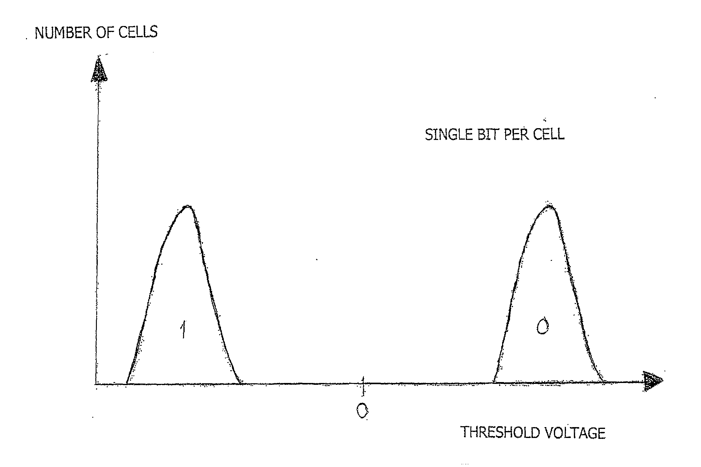
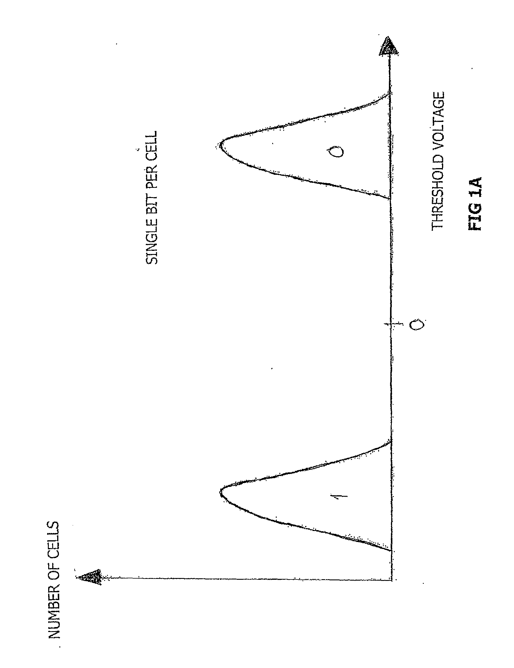
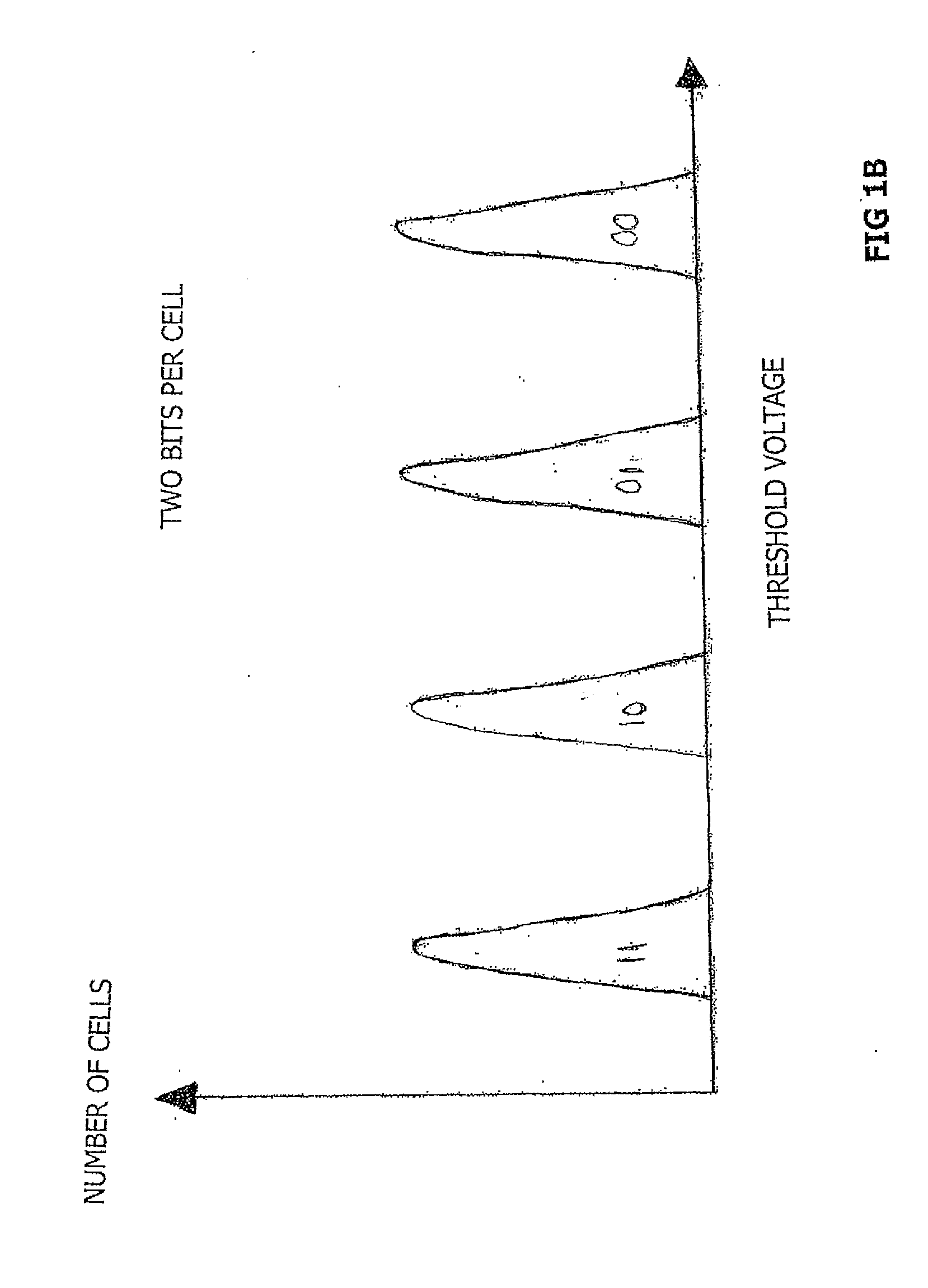
FIELD AND BACKGROUND OF THE INVENTION[0001]The present invention relates to memory devices such as flash memory devices and, more particularly, to a memory device whose controller exports a logical sector-based interface.[0002]Flash memory devices have been known for many years. Typically, each cell within a flash memory stores one bit of information. Traditionally, the way to store a bit has been by supporting two states of the cell—one state represents a logical “0” and the other state represents a logical “1”. In a flash memory cell the two states are implemented by having a floating gate above the cell's channel (the area connecting the source and drain elements of the cell's transistor), and having two valid states for the amount of charge stored within this floating gate. Typically, one state is with zero charge in the floating gate and is the initial unwritten state of the cell after being erased (commonly defined to represent the “1” state) and another state is with some amo...

Claims


Application Information

Patent Timeline
IPC IPC(8): G06F12/00
CPCG06F2212/7201G06F12/0246
Inventor LASSER, MENAHEM
Owner LASSER MENAHEM
Learn More