Defect prevention on SRAM cells that incorporate selective epitaxial regions

a selective epitaxial region and defect prevention technology, applied in the field of sram devices, can solve the problems of degrading electrical characteristics, affecting the mobility or drive current of carriers, and extremely thin epitaxial layers, so as to improve the mobility or drive current, reduce defects, and improve the effect of carrier mobility

Active Publication Date: 2013-08-01
TEXAS INSTR INC
View PDF1 Cites 0 Cited by
  • Summary
  • Abstract
  • Description
  • Claims
  • Application Information

AI Technical Summary

Benefits of technology

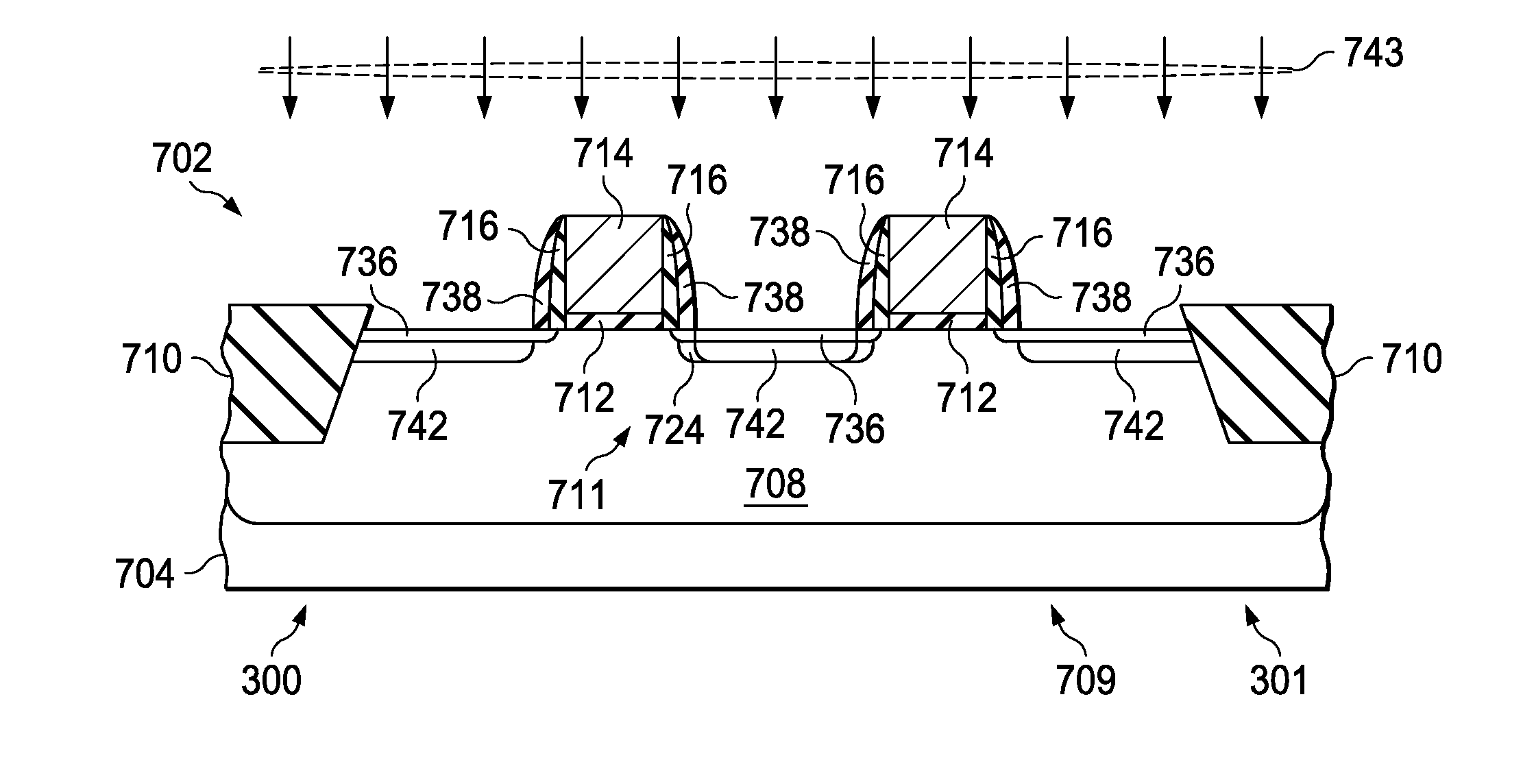
The present invention describes a device and method of fabrication that improves the mobility and drive current of MOS transistors in an SRAM memory device. This is achieved by applying stress to the channel region of the transistors, which leads to increased carrier mobility without causing a significant number of defects. The fabrication process also protects the moat tip regions of the PMOS transistors from damage during etching and selective epitaxial growth. Additionally, the invention includes a method of selectively growing epitaxial silicon germanium material in the semiconductor body to induce strain in the channel region. This results in more effective strain translation to the channel and reduces defects associated with selective epitaxial growth in moat tip regions. Overall, this invention enhances the performance and reliability of SRAM memory devices.

Problems solved by technology

However, advanced SRAM devices have a tendency to produce various defects associated with selective epitaxial growth in moat tip regions.
These defects are due to the reduced dimensions of the region, preventing proper epitaxial growth and resulting in extremely thin epitaxial layers.
Such defects also result in degraded electrical characteristics, degraded contacts and silicide formation, and poor diode characteristics.
In addition, transistors fabricated with selective epitaxial regions in the source / drains suffer from high off-state current due to subsurface leakage.

Method used


Image

  • Defect prevention on SRAM cells that incorporate selective epitaxial regions
  • Defect prevention on SRAM cells that incorporate selective epitaxial regions
  • Defect prevention on SRAM cells that incorporate selective epitaxial regions

Examples


Embodiment Construction

[0028]One or more implementations of the present invention will now be described with reference to the attached drawings, wherein like reference numerals are used to refer to like elements throughout, and wherein the illustrated structures are not necessarily drawn to scale. The invention provides transistor and SRAM memory structures and methods in which transistor mobility or drive current is improved while minimizing defects associated with selective epitaxial growth in moat tip regions of the core region of such memory devices.

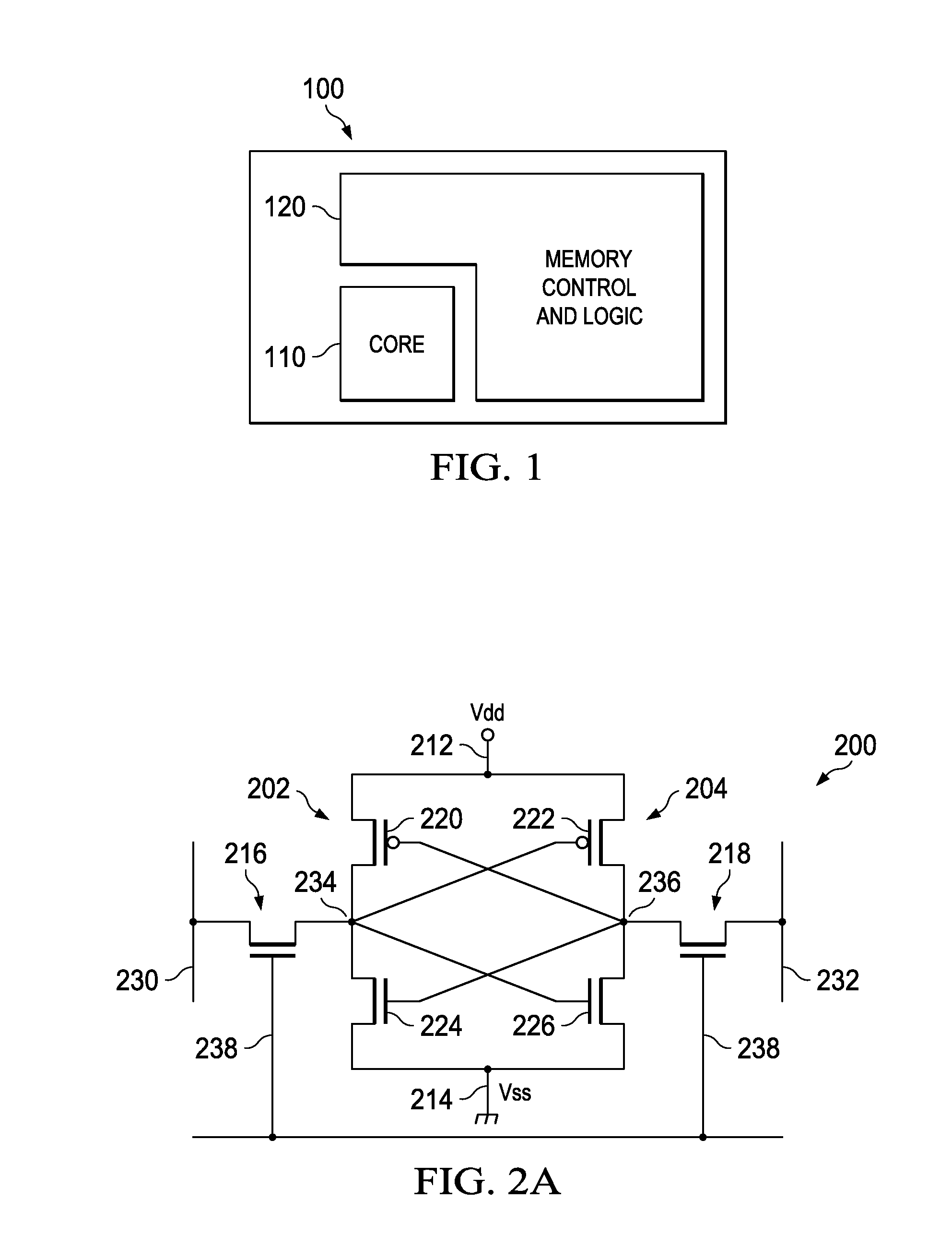
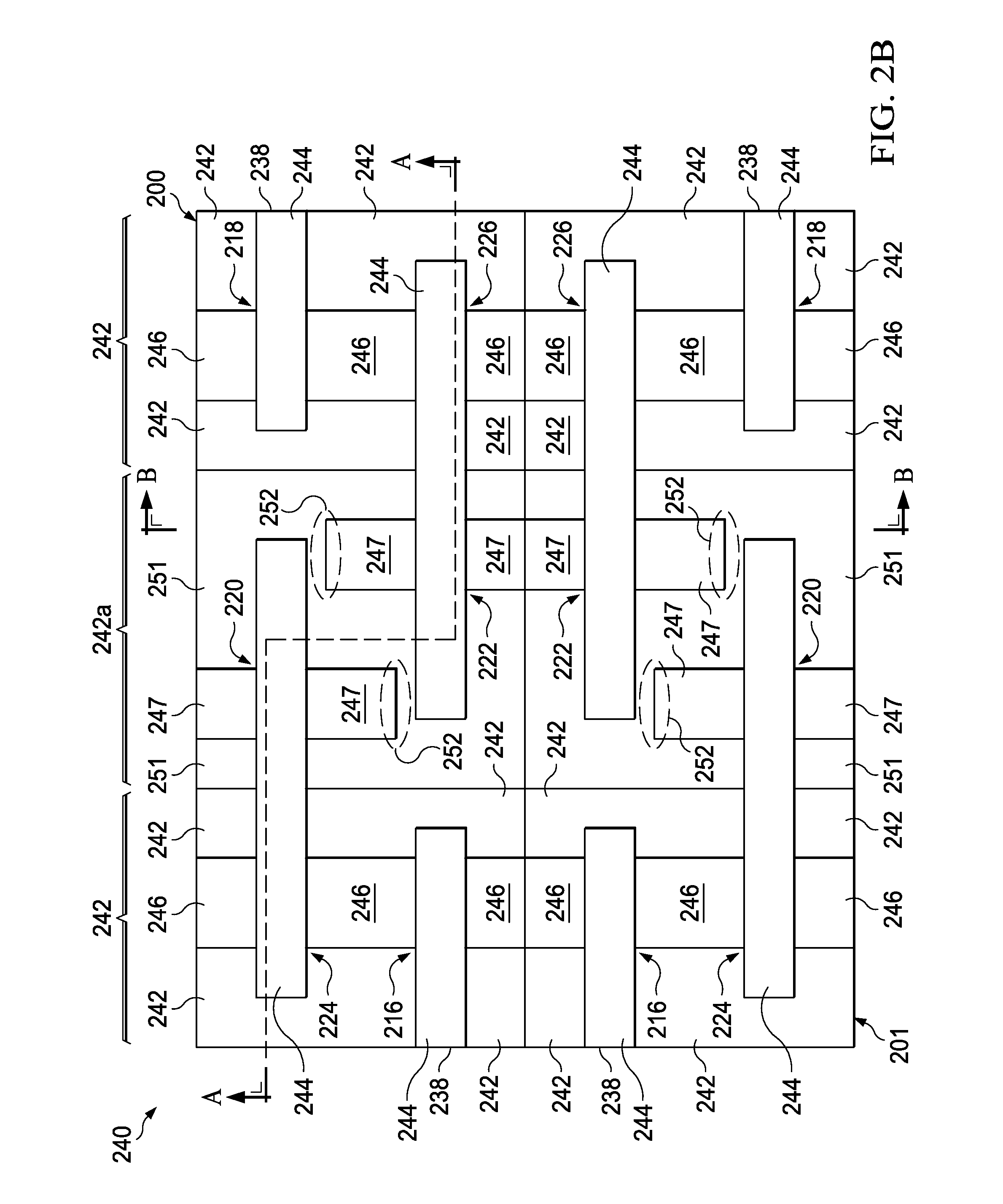
[0029]Referring now to FIG. 1, an exemplary semiconductor device that incorporates SRAM memory circuitry 100 is illustrated such as may be used in accordance with one or more aspects of the present invention. The SRAM memory containing device 100 comprises, for example, a semiconductor integrated circuit chip having a core region 110 and a logic region 120. The core region 110 comprises an array of SRAM memory cells, for example, an array of 6T SRAM memory...


PUM


Abstract

An SRAM device and method of forming MOS transistors of the device having reduced defects associated with selective epitaxial growth in moat tip regions is discussed. The SRAM device comprises a core region and a logic region, logic transistors within the logic region of the SRAM, and selective epitaxial regions grown on both source and drain regions; and memory cell transistors within the core region of the SRAM, and having the selective epitaxial regions grown on only one of the source and drain regions. One method of forming the MOS transistors of the SRAM cell comprises forming a gate structure over a first conductivity type substrate to define a channel therein, masking one of the source and drain regions in the core region, forming a recess in the substrate of the unmasked side of the channel, epitaxially growing SiGe in the recess, removing the mask, and forming the source and drain extension regions in source / drain regions.

Description

CROSS-REFERENCE TO RELATED APPLICATIONS[0001]This application is a divisional of U.S. patent application Ser. No. 11 / 453,190, entitled “DEFECT PREVENTION ON SRAM CELLS THAT INCORPORATE SELECTIVE EPITAXIAL REGIONS,” filed on Jun. 14, 2006 (now U.S. Pat. No. ______), which is incorporated herein by reference for all purposes.FIELD OF INVENTION[0002]The present invention relates generally to semiconductor devices and more particularly to static random access memory (SRAM) devices and associated methods of manufacture having reduced defects associated with selective epitaxial growth in moat tip regions, and improved low leakage transistors having improved mobility due to channel strain.BACKGROUND OF THE INVENTION[0003]A conventional MOS transistor generally includes a semiconductor substrate, such as silicon, having a source, a drain, and a channel positioned between the source and drain. A gate stack composed of a conductive material (a gate conductor), an oxide layer (a gate oxide), a...

Claims


Application Information

Patent Timeline
Patent Type & Authority Applications(United States)
IPC IPC(8): H01L29/66
CPCH01L21/823412H01L21/823418H01L27/088H01L29/66477H01L27/1104H01L29/66636H01L29/7848H01L27/11H10B10/00H10B10/12
Inventor ROTONDARO, ANTONIO L.
Owner TEXAS INSTR INC
Why Eureka
Try Eureka