Organic light emitting display device and method for fabricating the same

a technology of light-emitting display and organic materials, which is applied in the direction of thermoelectric device junction materials, semiconductor devices, electrical apparatus, etc., can solve the problems of increasing fabrication costs and process time, and achieve the effects of reducing the number of masks, reducing fabrication costs, and simplifying the fabrication process

Active Publication Date: 2013-08-15
LG DISPLAY CO LTD
View PDF4 Cites 40 Cited by
  • Summary
  • Abstract
  • Description
  • Claims
  • Application Information

AI Technical Summary

Benefits of technology

[0014]Accordingly, the present invention provides an organic light emitting display device and a method for fabricating the same capable of simultaneously forming an oxide semiconductor layer and a first electrode an...

Problems solved by technology

That is, the conventional OLED device as described above is fabricated using eighth masks up ...

Method used


Image

  • Organic light emitting display device and method for fabricating the same
  • Organic light emitting display device and method for fabricating the same
  • Organic light emitting display device and method for fabricating the same

Examples


first embodiment

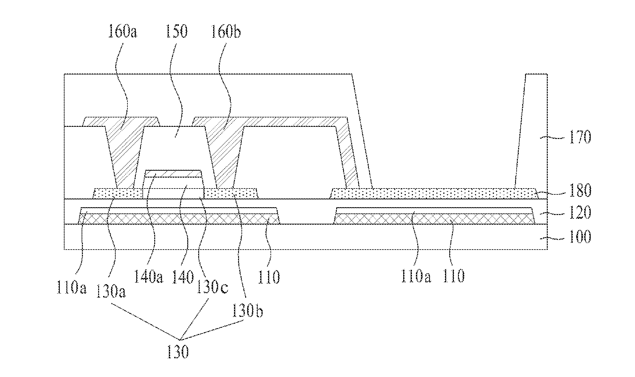
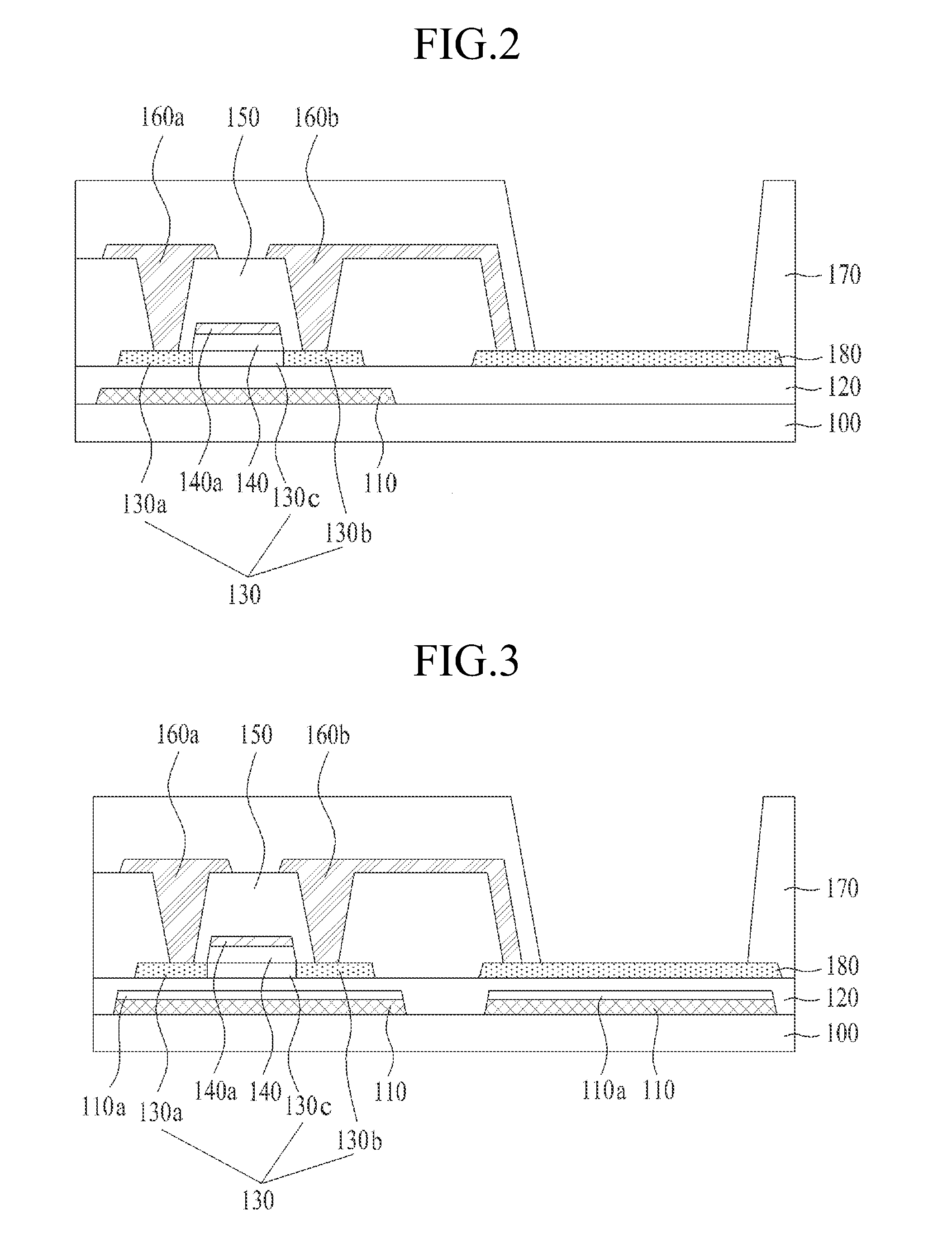
[0068]FIGS. 6A to 6E are sectional views for specifically explaining the plasma treatment process and the third mask process illustrated in FIG. 5C.

[0069]As shown in FIG. 6A, a gate insulation material 220a and a gate electrode material 220b are deposited in turn on the surface of the substrate 100 formed with the oxide semiconductor layer 130. Then, a photoresist pattern 230 is formed on the gate electrode material 220b through a photolithographic process using a photo mask (not shown) such as a half tone mask and a slit mask. The photoresist pattern 230 having a first height is formed at a semi-transmission region P3 of the photo mask, whereas the photoresist pattern 230 having a greater second height than the first height is formed at a cut-off region P1 of the photo mask. Also, a transmission region P2 of the photo mask is formed to expose the gate electrode material 220b.

[0070]Through an etching process using the photoresist pattern 230 as a mask, the gate insulation and gate ...

second embodiment

[0074]FIGS. 7A to 7D are sectional views for specifically explaining the plasma treatment process and the third mask process illustrated in FIG. 5C.

[0075]As shown in FIG. 7A, a gate insulation material 220a and a gate electrode material 220b are deposited in turn on the entire surface of the substrate 100 formed with the oxide semiconductor layer 130. Then, a photoresist pattern 230 is formed on the gate electrode material 220b through a photolithographic process using a photo mask (not shown). The photoresist pattern 230 is formed at a cut-off region P1 of the photo mask, and a transmission region P2 of the photo mask is formed to expose the gate electrode material 220b.

[0076]The gate insulation and gate electrode materials 220a and 220b are etched through an etching process using the photoresist pattern 230 as a mask, as shown in FIG. 7B. Consequently, the gate insulation film 140 and gate electrode 140a having the same pattern are formed on the oxide semiconductor layer 130, and...


PUM


Abstract

An organic light emitting display device includes a light shield layer formed on a substrate and a buffer layer formed on an entire surface of the substrate, an oxide semiconductor layer and first electrode formed on the buffer layer, a gate insulation film and gate electrode formed on the oxide semiconductor layer while being deposited to expose both edges of the oxide semiconductor layer, an interlayer insulation film formed to expose both the exposed edges of the oxide semiconductor layer and the first electrode, source and drain electrodes connected with one edge and the other edge of the oxide semiconductor layer, respectively, and a protective film formed to cover the source and drain electrodes while exposing a region of the first electrode so as to define a luminescent region and a non-luminescent region.

Description

CROSS-REFERENCE TO RELATED APPLICATIONS[0001]This application claims priority to Republic of Korea Patent Application No. 10-2012-0013173, filed on Feb. 9, 2012, and to Republic of Korea Patent Application No. 10-2012-0119615, filed on Oct. 26, 2012, both of which are incorporated by reference herein in their entirety.BACKGROUND OF THE INVENTION[0002]1. Field of the Invention[0003]The present invention relates to an organic light emitting display device and a method for fabricating the same capable of simplifying a fabrication process.[0004]2. Discussion of the Related Art[0005]For an image display device which embodies a variety of information on a screen as a core technology in advanced information and communication, there is continuous progress in development of thin, light-weight, and portable devices with improved performance. Hereupon, an Organic Light Emitting Display (OLED) device for controlling a luminescent amount of an organic luminescent layer is recently receiving atte...

Claims


Application Information

Patent Timeline
IPC IPC(8): H01L51/56H01L27/32
CPCH01L27/3225H01L51/56H01L27/3248H01L27/1225H01L27/3262H01L29/78633H01L51/5284H10K59/123H10K59/1213H10K50/865H10K71/00H10K59/00
Inventor KIM, MIN-JOOJEONG, HO-YOUNG
Owner LG DISPLAY CO LTD
Why Eureka
Try Eureka