Printing phosphor on LED wafer using dry film lithography

a technology of phosphor and film lithography, which is applied in the manufacture of semiconductor/solid-state devices, electrical equipment, semiconductor devices, etc., can solve problems such as color shifting

Active Publication Date: 2013-08-15
LEDENGIN
View PDF4 Cites 23 Cited by
  • Summary
  • Abstract
  • Description
  • Claims
  • Application Information

AI Technical Summary

Benefits of technology

[0006]Embodiments of the present invention relate to methods for placing controlled amount of phosphor-containing material on top of LED dies formed on a substrate, such as a semiconductor wafer. A patterned photoresist can be used to mask out areas of the wafer and the LED dies where no phosphor-containing material is desired. In some embodiments, the phosph

Problems solved by technology

One drawback of this method is that the liquid mixt

Method used


Image

  • Printing phosphor on LED wafer using dry film lithography
  • Printing phosphor on LED wafer using dry film lithography
  • Printing phosphor on LED wafer using dry film lithography

Examples


Embodiment Construction

[0030]The description below will be made with reference to a series of drawing figures enumerated above. These diagrams are merely examples, and should not unduly limit the scope of the claims herein. In connection with the various aspects illustrated and described, one of ordinary skill in the art would recognize other variations, modifications, and alternatives.

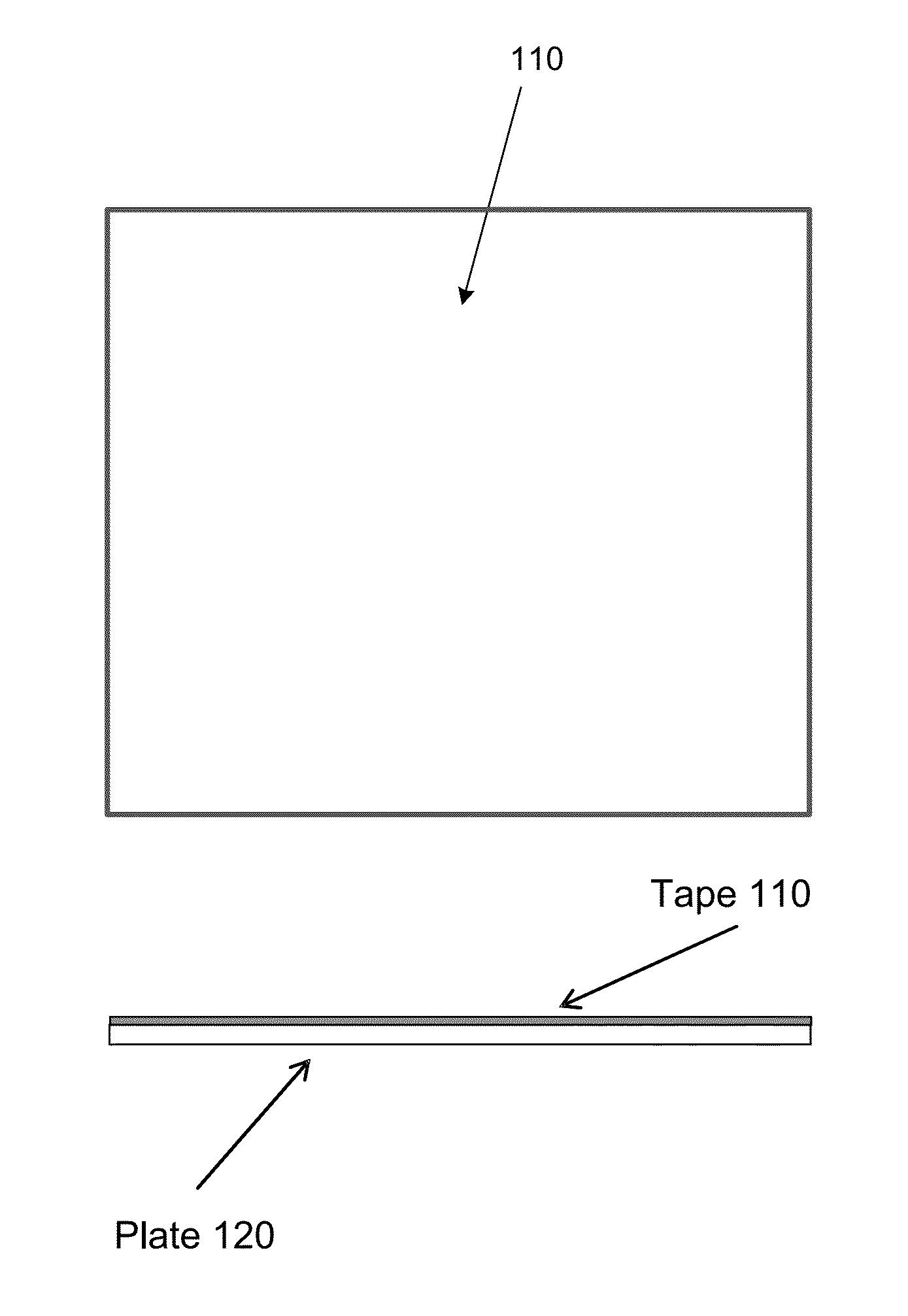
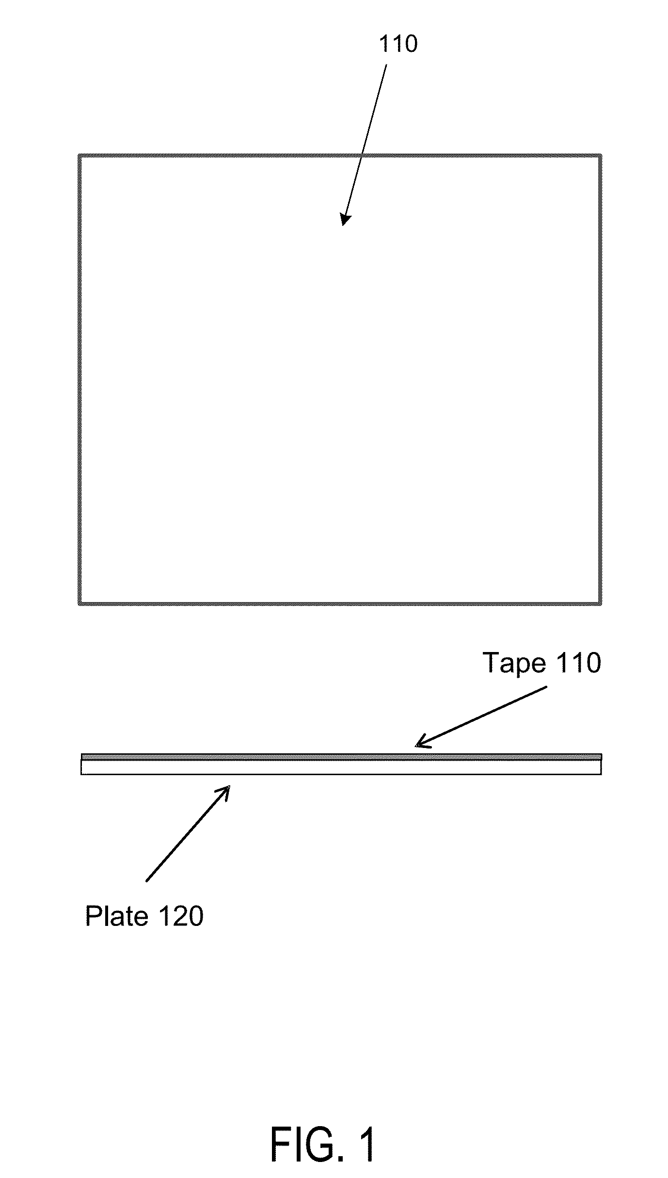
[0031]FIG. 1 shows a top view and a cross-sectional view of a substrate for carrying out the method for phosphor deposition. An adhesive tape 110 is disposed on a glass plate 120. In an embodiment, the tape is a double-sided adhesive tape, which can be a thermal release or a UV release tape made of, e.g., polyester. For example, a commercially available tape from Semiconductor Equipment Corp. can be used. Tape 110 is attached to plate 120 the glass substrate. In a specific embodiment, plate 120 is about 1 mm thick. But plates having other suitable thicknesses can also be used.

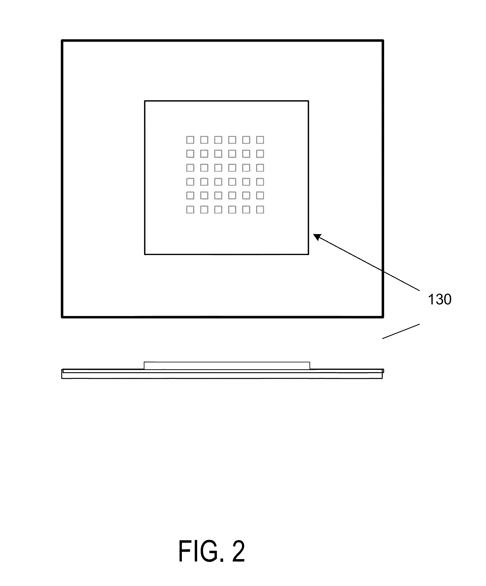
[0032]In FIG. 2, a grid template 130 is disposed...


PUM


Abstract

A method for depositing a layer of phosphor-containing material on a plurality of LED (light-emitting diode) dies on a wafer includes disposing a layer of dry photoresist film over a plurality of LED dies on a wafer, disposing a mask layer over the dry photoresist film, and patterning the dry photoresist film to form a plurality of openings in the dry photoresist film to expose a top surface of each of the LED dies. The method also includes depositing a phosphor-containing material on the exposed top surface of each the LED dies using a screen printing process, and removing the patterned dry photoresist film.

Description

CROSS-REFERENCES TO RELATED APPLICATIONS[0001]This application is a continuation-in-part of U.S. patent application Ser. No. 13 / 338,936, Attorney Docket No. 91924-001700US-80856, filed Dec. 28, 2011, commonly owned and incorporated herein by reference in its entirety.[0002]This application is also related to U.S. patent application Ser. No. 13 / 338,912, Titled Attorney Docket No. 91924-001600US-808563, filed Dec. 28, 2011, and U.S. patent application Ser. No. 13 / 714,399, Attorney Docket No. 91924-02500US-808563, filed Dec. 13, 2012, both of which are commonly owned and incorporated herein by reference in its entirety.BACKGROUND OF THE INVENTION[0003]The present invention relates in general to light-emitting diodes (LEDs) and in particular to deposition of phosphor-containing material on LED dies on a wafer.[0004]With the incandescent light bulb producing more heat than light, the world is eager for more efficient sources of artificial light. LEDs are a promising technology and are al...

Claims


Application Information

Patent Timeline
IPC IPC(8): H01L33/50
CPCH01L33/508H01L33/505H01L33/50H01L2933/0041
Inventor MEI, ZEQUNYAN, XIANTO
Owner LEDENGIN
Why Eureka
Try Eureka