Control for automated soldering

a technology of automated soldering and control, which is applied in the direction of program control, soldering apparatus, instruments, etc., can solve the problems of difficult to the difficulty of using a conventional selective wave soldering solution on such a formed bus bar, and the inability to easily control the vertical position of each soldering joint. achieve the effect of superior soldering joints

Active Publication Date: 2013-08-15
TESLA INC
View PDF13 Cites 4 Cited by
  • Summary
  • Abstract
  • Description
  • Claims
  • Application Information

AI Technical Summary

Benefits of technology

[0011]Features / benefits include an ability to precisely variably locate a mobile solder wave vertically allowing embodiments of the present invention to uniformly provide superior solder joints over conventional selective wave solder systems and the like. Any warpage in a foundation structure supporting the electronic devices to be soldered is compensated for automatically.

Problems solved by technology

It is not uncommon to have relatively large arrays of devices, and in such a context the conventional selective wave soldering solution is not always able to easily control a vertical position of each solder joint within a sufficient level of precision to allow repeatable solder joints.
These bus bars may have height deviations that can cause solder joint locations to vary widely.
Using a conventional selective wave soldering solution on such a formed bus bar is problematic as solder joint location is not tightly controlled in wave height.

Method used


Image

  • Control for automated soldering
  • Control for automated soldering
  • Control for automated soldering

Examples


Embodiment Construction

[0019]Embodiments of the present invention provide an apparatus, method, and computer-program product for controlling fine positioning in a robotic electronic array processor, particularly a selective wave soldering station. The following description is presented to enable one of ordinary skill in the art to make and use the invention and is provided in the context of a patent application and its requirements.

[0020]Various modifications to the preferred embodiment and the generic principles and features described herein will be readily apparent to those skilled in the art. Thus, the present invention is not intended to be limited to the embodiment shown but is to be accorded the widest scope consistent with the principles and features described herein.

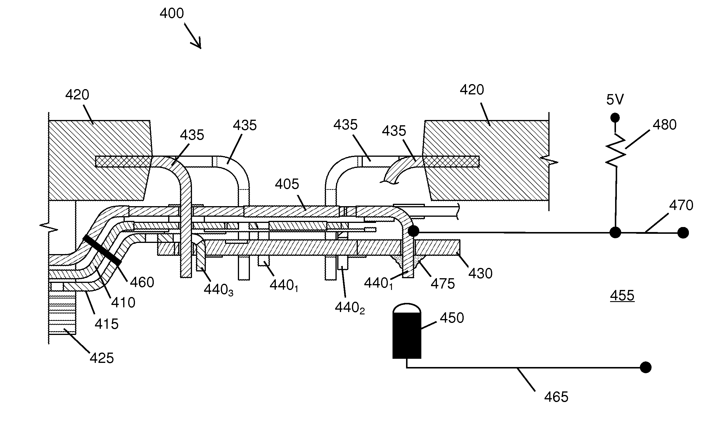
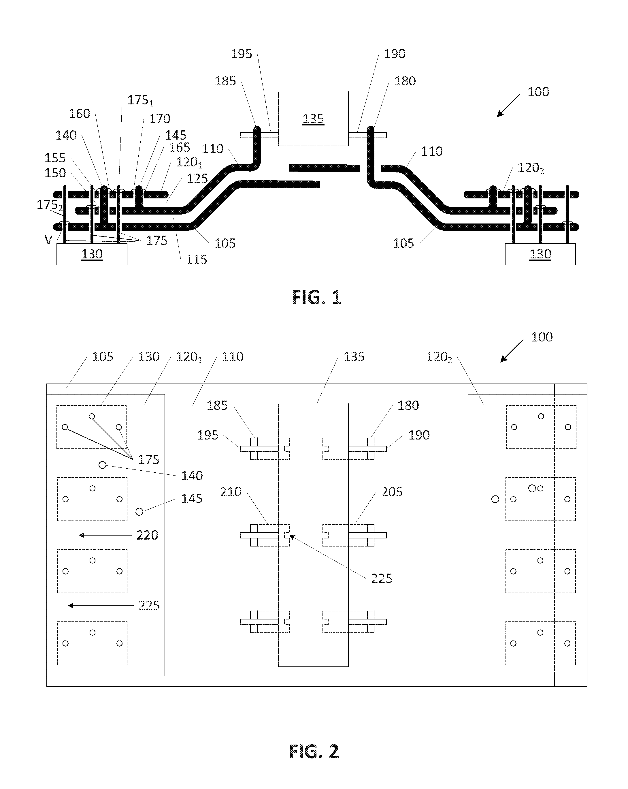
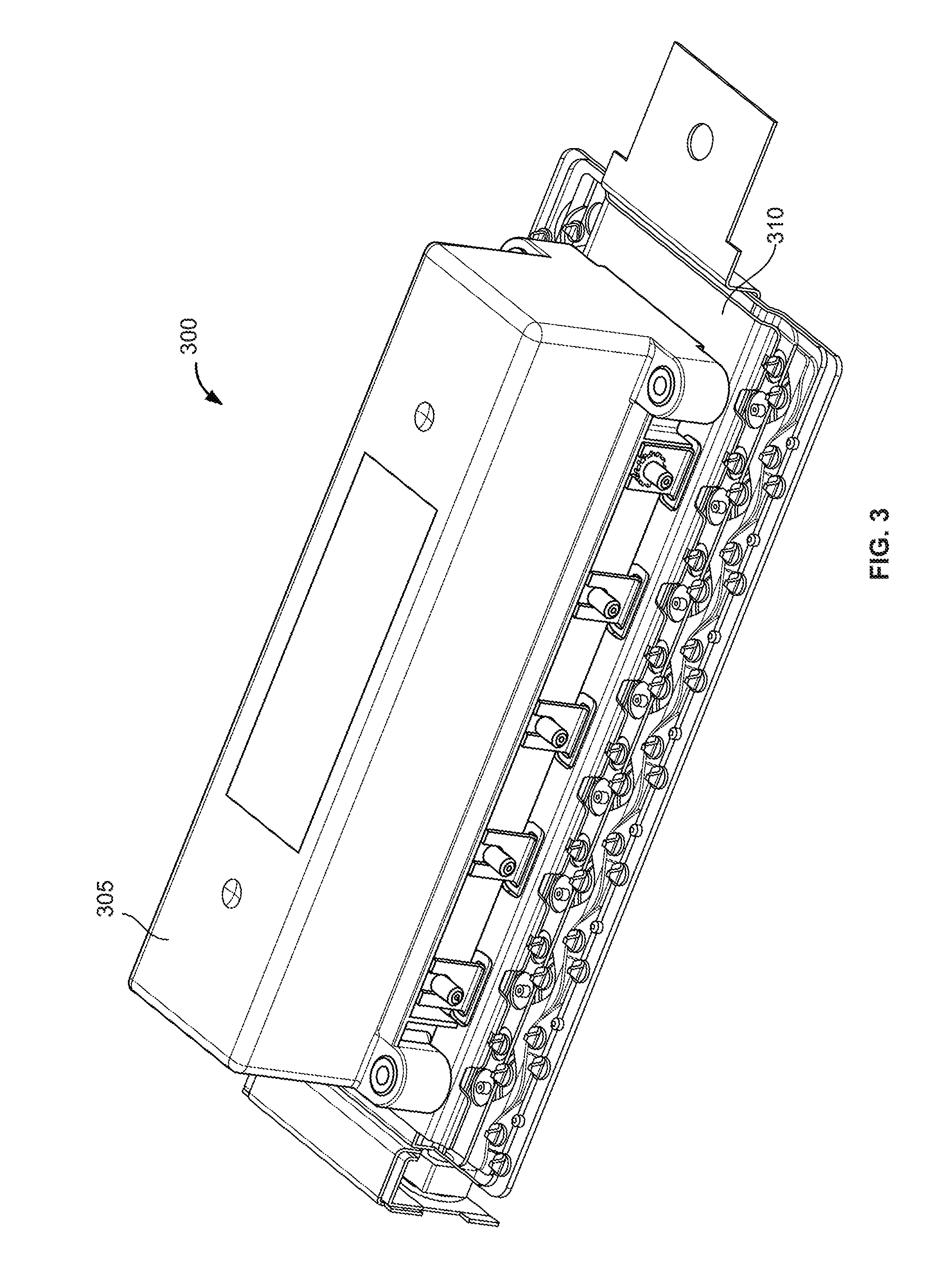
[0021]As noted above, an exemplary embodiment of the present invention processes a formed bus bar and the like. FIG. 1 illustrates a block schematic representation of an end-view of a formed bus bar 100. Bus bar 100 includes a pluralit...


PUM

PropertyMeasurementUnit
thicknessesaaaaaaaaaa
voltageaaaaaaaaaa

Abstract

A robotic processing system includes a microprocessor-controlled workpiece processor having a mobile processing element to be positioned independently in three orthogonal dimensions with respect to each of a plurality of target locations on a workpiece, with each particular target location of the plurality of target locations including an element to be processed, the mobile processing element processing the element at each particular target location by first moving to an initial location that is offset from the particular target location in a single dimension and then second moving along the single dimension towards the element at the particular target location until a contact signal is detected; and a control, coupled to the workpiece and to the mobile processing element, communicating the contact signal to the workpiece processor when the processing element makes physical contact with the element at the particular target location.

Description

BACKGROUND OF THE INVENTION[0001]The present invention relates generally to control of robotic systems, and more particularly but not exclusively, to closed loop control for soldering systems.[0002]For some arrangements and configurations of semiconductor devices disposed on printed circuit board assemblies, formed bus bars and the like, the use of soldered joints provide mechanical and electrical interconnection. One tool for making such solder joints is a selective wave soldering station. This tool includes a mobile solder pot controlled in three-dimensions to locate a standing solder wave at each solder joint location such that solder contact is made at the target joint location.[0003]It is not uncommon to have relatively large arrays of devices, and in such a context the conventional selective wave soldering solution is not always able to easily control a vertical position of each solder joint within a sufficient level of precision to allow repeatable solder joints.[0004]As an e...

Claims


Application Information

Patent Timeline
Patent Type & Authority Applications(United States)
IPC IPC(8): B23K1/002B25J13/08B25J9/06
CPCB23K3/0653
Inventor KALAYJIAN, NICHOLAS ROBERT
Owner TESLA INC
Why Eureka
Try Eureka