

Radiation detection apparatus
- Summary
- Abstract
- Description
- Claims
- Application Information
AI Technical Summary
Benefits of technology
Problems solved by technology
Method used
Image

Examples
first embodiment
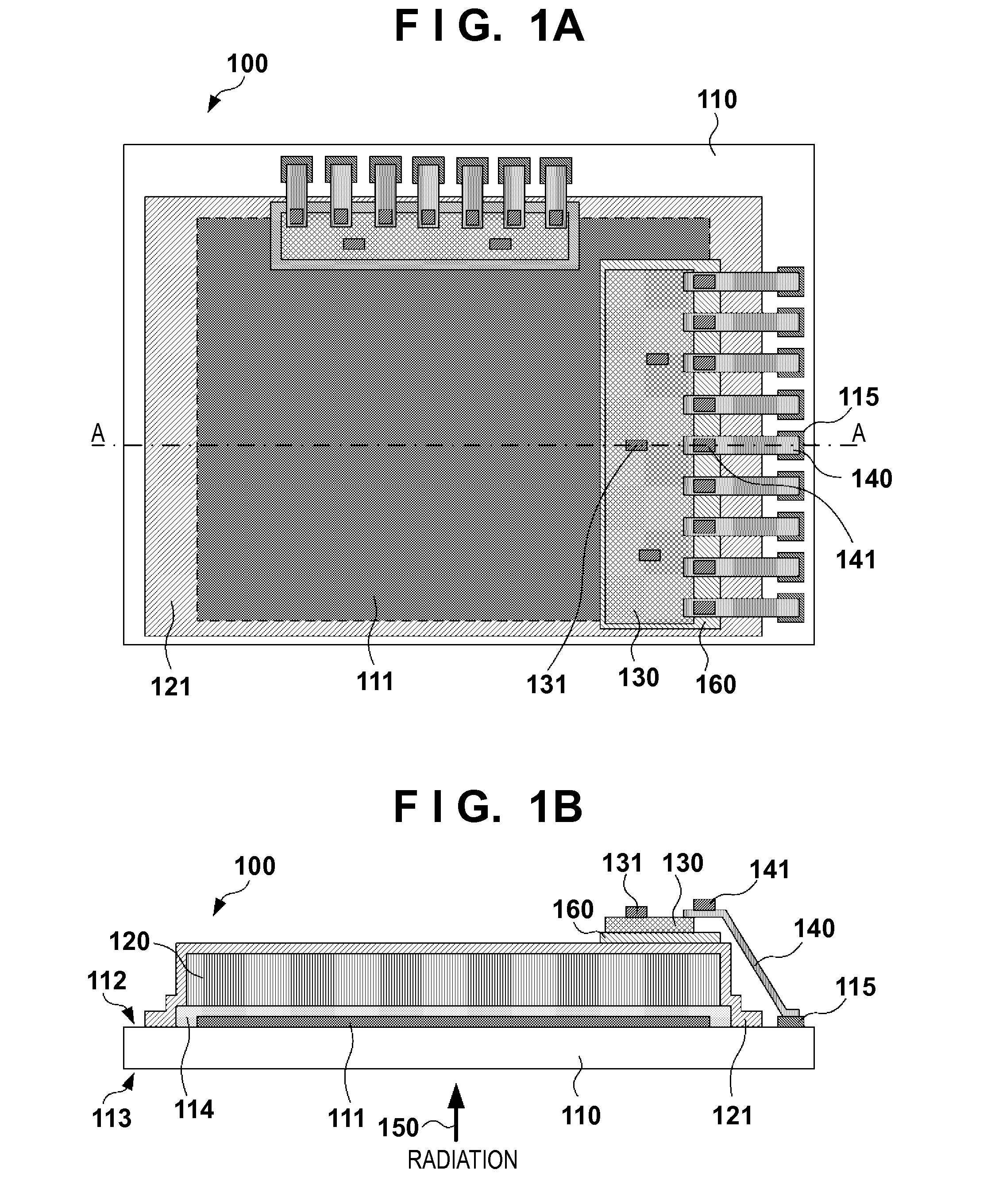
[0013]An example of a structure of a sensor unit 100 according to the present invention will now be described with reference to FIGS. 1A and 1B. The sensor unit 100 may be used as part of a radiation detection apparatus, as described later. FIG. 1A is a plan view of the sensor unit 100, and FIG. 1B is a cross-sectional view taken along the line A-A in FIG. 1A. The sensor unit 100 can mainly include a sensor substrate 110, a scintillator layer 120, a circuit board 130, and a connection portion 140. Although FIG. 1A shows a pixel array 111 for illustrative purposes, the pixel array 111 cannot actually be viewed since it is disposed under a scintillator protection layer 121.
[0014]The pixel array 111 is formed on one surface (a first surface) of the sensor substrate 110. In the following description, the surface on which the pixel array 111 is formed is referred to as a light-receiving surface 112, and an opposite surface (a second surface) is referred to as a radiation-entrance surface...
second embodiment
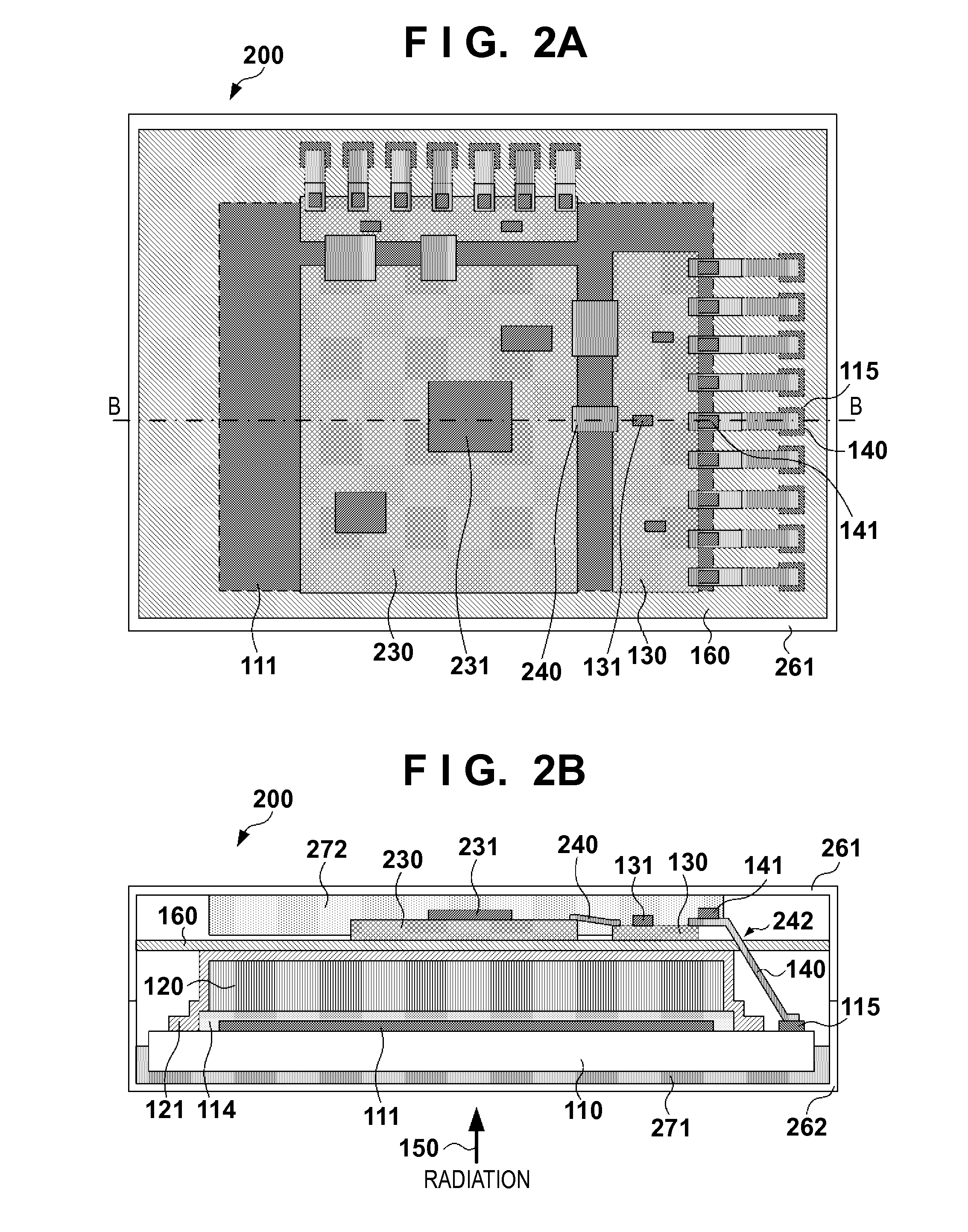
[0026]An example of a structure of a radiation detection apparatus 200 according to the present invention will now be described with reference to FIGS. 2A and 2B. FIG. 2A is a plan view of the radiation detection apparatus 200, and FIG. 2B is a cross-sectional view taken along the line B-B in FIG. 2A. The radiation detection apparatus 200 can mainly include a sensor unit and a cover for accommodating and protecting the sensor unit. Since the sensor unit of the radiation detection apparatus 200 has the similar configuration as that of the sensor unit 100 illustrated in FIGS. 1A and 1B, the same reference numerals are given to components that are same as those described with reference to FIGS. 1A and 1B, and any duplicated descriptions thereof are omitted. In FIG. 2A, for illustrative purposes, the upper surface of the cover is omitted. The pixel array 111, part of the connection portion 140, and the connection terminal 115, which are shown in FIG. 2A, cannot actually be viewed since ...
third embodiment
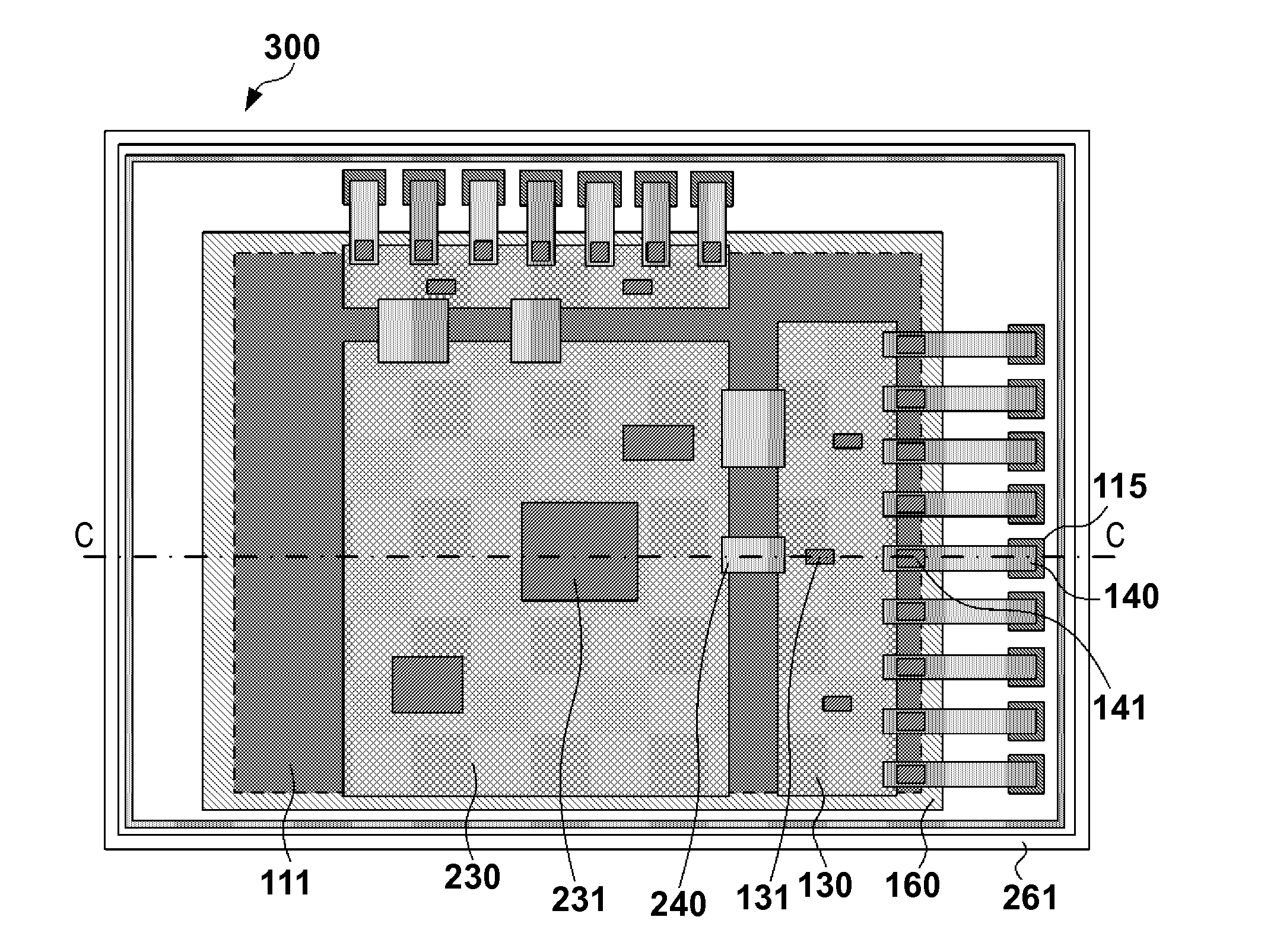
[0031]An example of a structure of a radiation detection apparatus 300 according to the present invention will now be described with reference to FIGS. 3A and 3B. FIG. 3A is a plan view of the radiation detection apparatus 300, and FIG. 3B is a cross-sectional view taken along the line C-C in FIG. 3A. The following will focus on the difference between the radiation detection apparatus 300 and the radiation detection apparatus 200, and any duplicated descriptions therebetween are omitted.
[0032]The radiation detection apparatus 300 is a radiation detection apparatus produced by an indirect method, in which a sensor panel and a scintillator panel are separately prepared, and then bonded to each other. The electromagnetic shield layer 160 may also serve as a scintillator substrate on which a scintillator is vapor deposited. With this measure, it is possible to achieve better weight reduction and minimization compared with the case where a scintillator substrate and an electromagnetic sh...
PUM
 Abstract
Description
Claims
Application Information