Method of forming nitrogen-free dielectric Anti-reflection layer

a dielectric anti-reflection and nitrogen-free technology, applied in the field of semiconductor manufacturing technology, can solve the problems that the standing wave effect, the poisoning effect of the photoresist, and the poor photoresist shape cannot be eliminated effectively, so as to reduce the extinction coefficient and the refractive index of the nitrogen-free dielectric anti-reflection layer effectively, and eliminate the photoresist standing wave effect.

Inactive Publication Date: 2013-08-29
SHANGHAI HUALI MICROELECTRONICS CORP
View PDF5 Cites 0 Cited by
  • Summary
  • Abstract
  • Description
  • Claims
  • Application Information

AI Technical Summary

Benefits of technology

[0017]According to the method of forming a nitrogen-free dielectric anti-reflection layer, when the process of introducing the reaction gas is performed prior to the process of generating the plasma, the content of silicon in the whole reaction chamber increases at the early stage so as to enhance the extinction coefficient and the refractive index of the nitrogen-free dielectric anti-reflection layer effectively. On the other hand, when the process of introducing the reaction gas is performed after the process of generating the plasma, the content of silicon in the whole r

Problems solved by technology

If the process of introducing the reaction gas and generating a plasma are performed at the same time with no time delay, it is difficult to control the refractive index and the extinction coefficient of th

Method used


Image

  • Method of forming nitrogen-free dielectric Anti-reflection layer
  • Method of forming nitrogen-free dielectric Anti-reflection layer
  • Method of forming nitrogen-free dielectric Anti-reflection layer

Examples


Embodiment Construction

[0021]A method of forming a nitrogen-free dielectric anti-reflection layer will be described in further details hereinafter with respect to the embodiment of the present invention and the accompanying drawings.

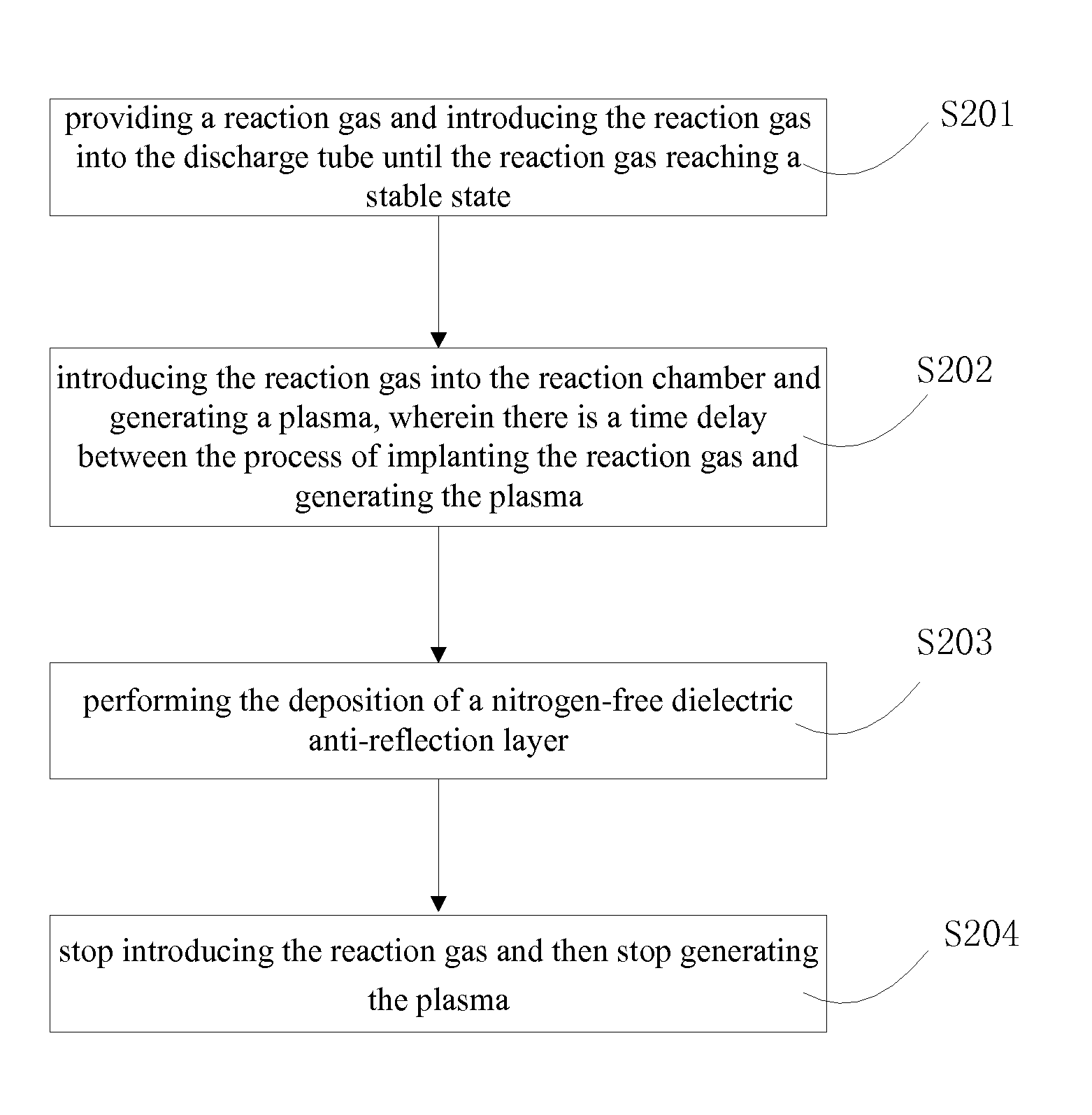
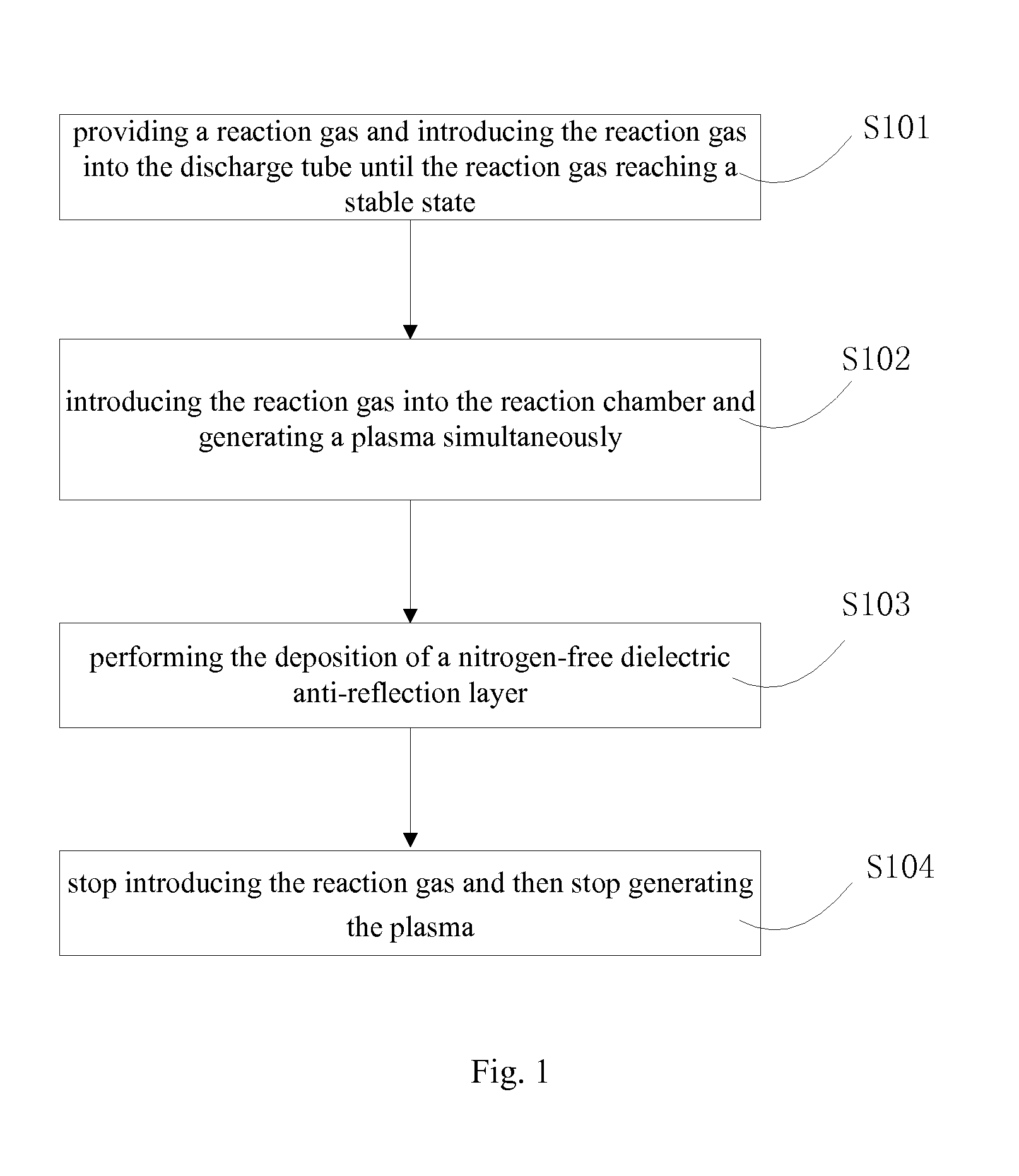
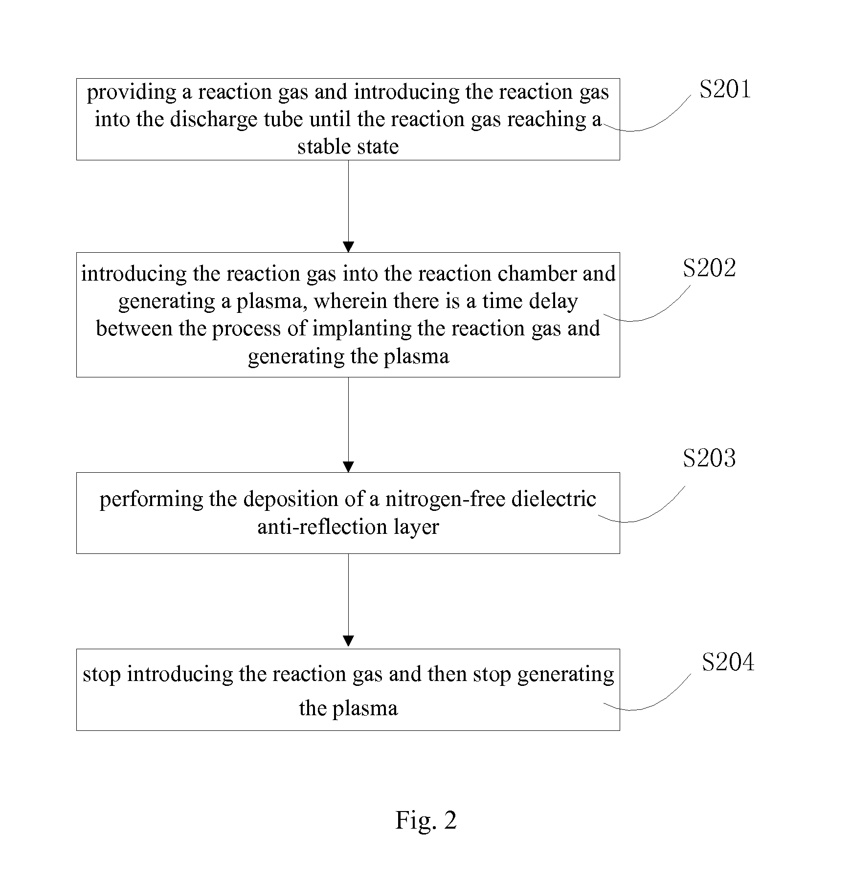
[0022]Referring to FIG. 2, a method of forming a nitrogen-free dielectric anti-reflection layer in the embodiment comprises the following steps:

[0023]Step S201, first providing a reaction gas, wherein the reaction gas can be a mixed gas of silane and carbon dioxide accompanied by some auxiliary gases such as helium or other inert gases. Then, introducing the reaction gas into a discharge tube until the reaction gas reaching a stable state; the flow rate of the reaction gas maintains stable.

[0024]Step S202, introducing the reaction gas into the reaction chamber and generating a plasma. There is a time delay between the process of introducing gas and the process of generating the plasma. Preferably, the time delay is in the range of 0.1 to 2 seconds. When the process of introduc...


PUM

PropertyMeasurementUnit
Timeaaaaaaaaaa
Timeaaaaaaaaaa
Pressureaaaaaaaaaa

Abstract

The present invention provides a method of forming a nitrogen-free dielectric anti-reflection layer comprising: introducing a reaction gas into the discharge tube until the reaction gas reaching a stable state; introducing the reaction gas into the reaction chamber and then generating a plasma, or generating a plasma and then introducing the reaction gas into the reaction chamber, wherein the time delay occurs between the two processes is utilized to perform the deposition of the nitrogen-free dielectric anti-reflection layer; finally stop introducing the reaction gas and then stop generating the plasma. The method can flexibly control the extinction coefficient and the refractive index of the nitrogen-free dielectric anti-reflection layer so as to obtain a straight photoresist pattern and greatly reduce the photoresist standing waves effect and photoresist poisoning effect.

Description

CROSS-REFERENCE TO RELATED APPLICATION[0001]This application claims the priority benefit of China application serial no. 201210050770.8, filed Feb. 28, 2012. All disclosure of the China application is incorporated herein by reference.FIELD OF THE INVENTION[0002]The present invention relates to the field of semiconductor manufacturing technology, and particularly to a method of forming a nitrogen-free dielectric anti-reflection layer.BACKGROUND OF THE INVENTION[0003]Conventionally, nitrogen-free dielectric anti-reflection layers are formed by introducing plasma and reaction gas simultaneously. Referring to FIG. 1, a conventional process of forming a nitrogen-free dielectric anti-reflection layer comprises the following steps: Step S101, providing a reaction gas and introducing the reaction gas into the discharge tube until the reaction gas reaching a stable state; Step S102, introducing the reaction gas into the reaction chamber and generating a plasma simultaneously; Step S103, perf...

Claims


Application Information

Patent Timeline
IPC IPC(8): C23C16/50
CPCC23C16/50C23C16/45512
Inventor CHEN, CHIENWEICHANG, HSUSHENG
Owner SHANGHAI HUALI MICROELECTRONICS CORP
Why Eureka
Try Eureka