Memory device having an integrated two-terminal current limiting resistor

a resistor and memory device technology, applied in semiconductor devices, digital storage, instruments, etc., can solve the problems of insufficient resistance inability to use low-to-moderate mo films to form reliable non-volatile memory devices, and insufficient resistance of these mo films and/or the ratio of high-to-low resistance states to be of practical use within non-volatile memory devices. achieve the effect of reducing saturated current flow, preventing “on” and “ o

Active Publication Date: 2013-08-29
INTERMOLECULAR
View PDF4 Cites 1 Cited by
  • Summary
  • Abstract
  • Description
  • Claims
  • Application Information

AI Technical Summary

Benefits of technology

[0014]The measured current versus voltage plot of the resulting memory device with the integrated current limiting resistor exhibits a non-linear resistance curve, showing a linear current to voltage relationship at low voltage levels and a reduced saturated current flow at higher applied voltage levels. By tailoring the electrical characteristics of the current limiting resistor (e.g., the thickness (L) and resistivity (p) of the lightly doped material layer of the resistor structure), the value of the saturation current (IMAX) or compliance current (ICC) can be controlled

Problems solved by technology

However, as device dimensions shrink, scaling issues pose challenges for traditional nonvolatile memory technology.
Although such metal oxide (MO) films exhibit bistability, the resistance of these MO films and/or the ratio of the high-to-low resistance states is (are) often insufficient to be of practical use within a nonvolatile memory device.
Since the variation in the difference between the resistance states is related to the resistance of the resistive switching memory element, it is often hard to use a low resistance metal oxide film to form a reliable nonvolatile memory device.
For example, in a nonvolatile memory device having conductive lines formed of a relatively high resistance metal such as tungsten, the resistance of the conductiv

Method used


Image

  • Memory device having an integrated two-terminal current limiting resistor
  • Memory device having an integrated two-terminal current limiting resistor
  • Memory device having an integrated two-terminal current limiting resistor

Examples


examples

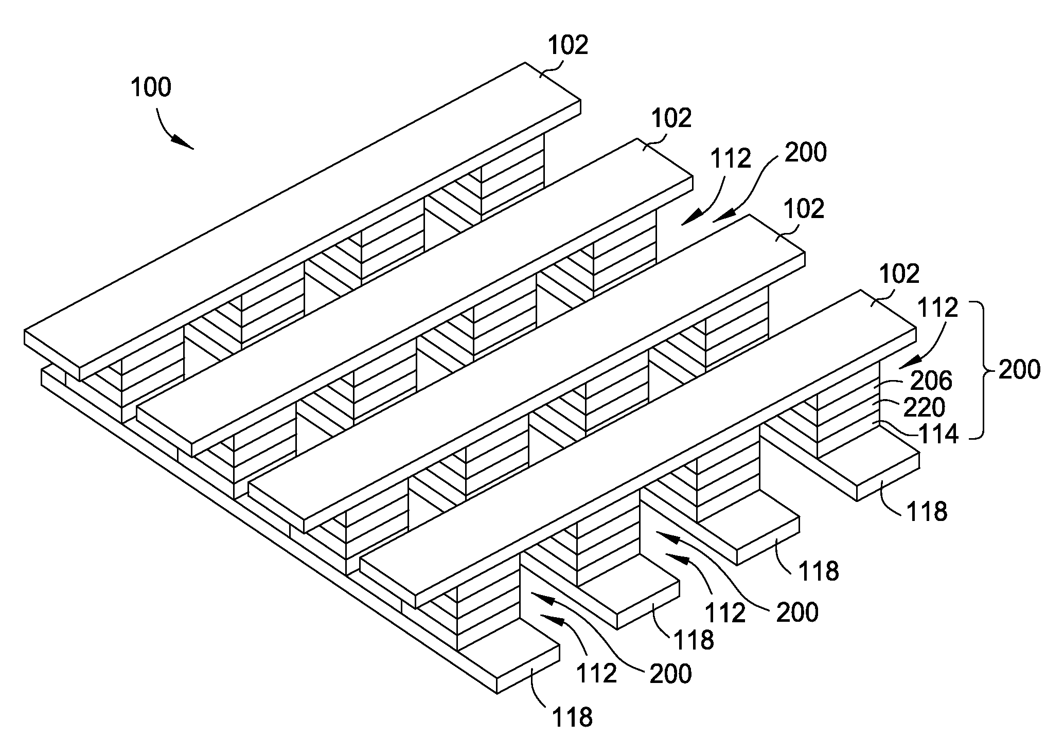
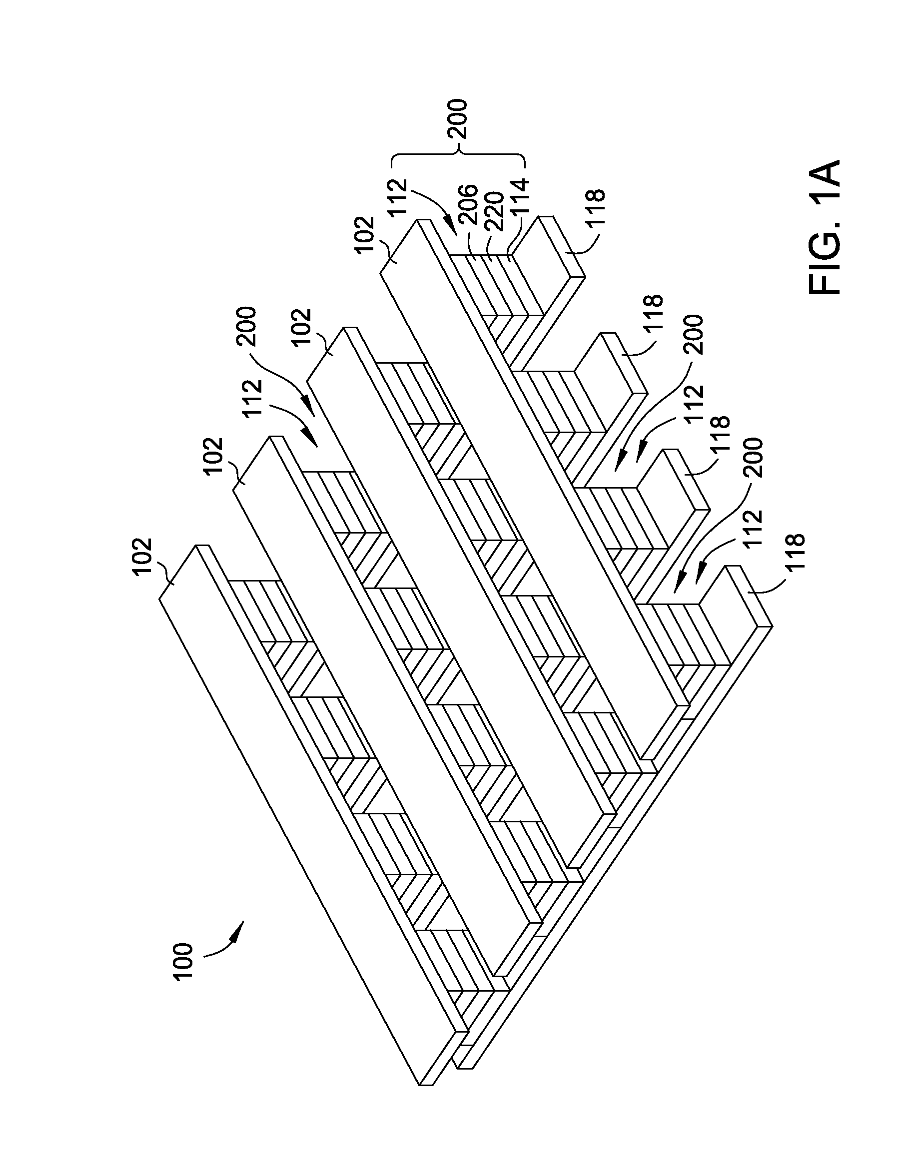
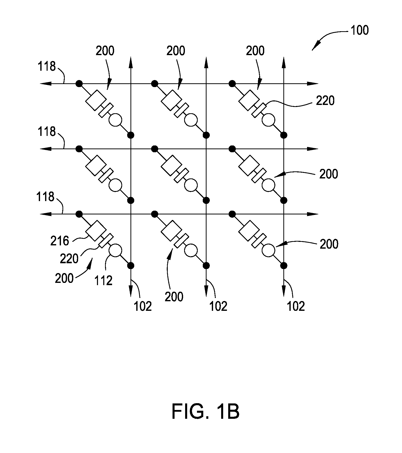
[0127]In one embodiment of a memory cell 200, after performing the processing sequence 700, the formed memory cell 200 comprises: about 50 Å of a titanium nitride (TiN) layer (as the electrode 102), about 30 Å thick of a hafnium oxide (HfOx) layer (as the variable resistance layer 206), about 50 Å thick of an n-doped polysilicon layer (as the intermediate electrode 210), and the resistor structure 220. The resistor structure 220 may be between about 10 Å and 1,000 Å thick and comprises a N+ polysilicon layer of between about 10 Å and 400 Å, a N− polysilicon layer of between about 10 Å and 500 Å, and a N+ polysilicon layer of between about 10 Å and 400 Å. After forming the memory cell 200 having the resistor structure and the resistive switching memory element 112 and other material layers, the formed memory cell 200 is subject to at least one thermal processing step to anneal and / or activate the material layers in the formed memory cell 200.

[0128]As an example, the memory cell 200 m...


PUM


Abstract

A resistor structure incorporated into a resistive switching memory cell or device to form memory devices with improved device performance and lifetime is provided. The resistor structure may be a two-terminal structure designed to reduce the maximum current flowing through a memory device. A method is also provided for making such memory device. The method includes depositing a resistor structure and depositing a variable resistance layer of a resistive switching memory cell of the memory device, where the resistor structure is disposed in series with the variable resistance layer to limit the switching current of the memory device. The incorporation of the resistor structure is very useful in obtaining desirable levels of device switching currents that meet the switching specification of various types of memory devices. The memory devices may be formed as part of a high-capacity nonvolatile memory integrated circuit, which can be used in various electronic devices.

Description

BACKGROUND OF THE INVENTION[0001]1. Field of the Invention[0002]This invention relates to the formation of resistive switching memory devices.[0003]2. Description of the Related Art[0004]Nonvolatile memory devices are used in systems in which persistent storage is required. For example, nonvolatile memory cards are used in digital cameras to store images and in digital music players to store audio data. Nonvolatile memory devices are also used to persistently store data in computer environments.[0005]Electrically-erasable programmable read only memory (EEPROM) technology is often used to form and program nonvolatile memory devices. This type of nonvolatile memory contains floating gate transistors that can be selectively programmed or erased by application of suitable voltages to their terminals. As fabrication techniques improve, it is becoming possible to fabricate nonvolatile memory devices with increasingly smaller dimensions. However, as device dimensions shrink, scaling issues...

Claims


Application Information

Patent Timeline
IPC IPC(8): H01L21/02
CPCH01L45/08H01L45/10H01L45/12H01L45/1233H01L45/14H01L27/2409H01L27/2463H01L45/16H01L45/146G11C13/0002G11C13/0007G11C13/003G11C13/004G11C13/0069G11C2013/0045G11C2013/0073G11C2013/0078G11C2013/0092G11C2213/76H10B63/20H10B63/80H10N70/25H10N70/801H10N70/24H10N70/826H10N70/8833H10N70/881H10N70/011
Inventor PRAMANIK, DIPANKARCHIANG, TONY P.LEE, MANKOO
Owner INTERMOLECULAR
Why Eureka
Try Eureka