Thin film resistor structure

Active Publication Date: 2013-09-12
UNITED MICROELECTRONICS CORP
View PDF8 Cites 43 Cited by
  • Summary
  • Abstract
  • Description
  • Claims
  • Application Information

AI Technical Summary

Benefits of technology

[0011]To summarize the above descriptions, the present invention provides a thin film resistor structure with a simplified manufacturing process compared to the conventional polysilicon resistor. Bes

Problems solved by technology

However, polysilicon materials have some drawbacks: the resistance of a polysilicon gate is higher than most of any metal materials, and the conductivity rate of the polysilicon gate is therefore lower than metal wires.
It is conceivable

Method used


Image

  • Thin film resistor structure
  • Thin film resistor structure
  • Thin film resistor structure

Examples


Example

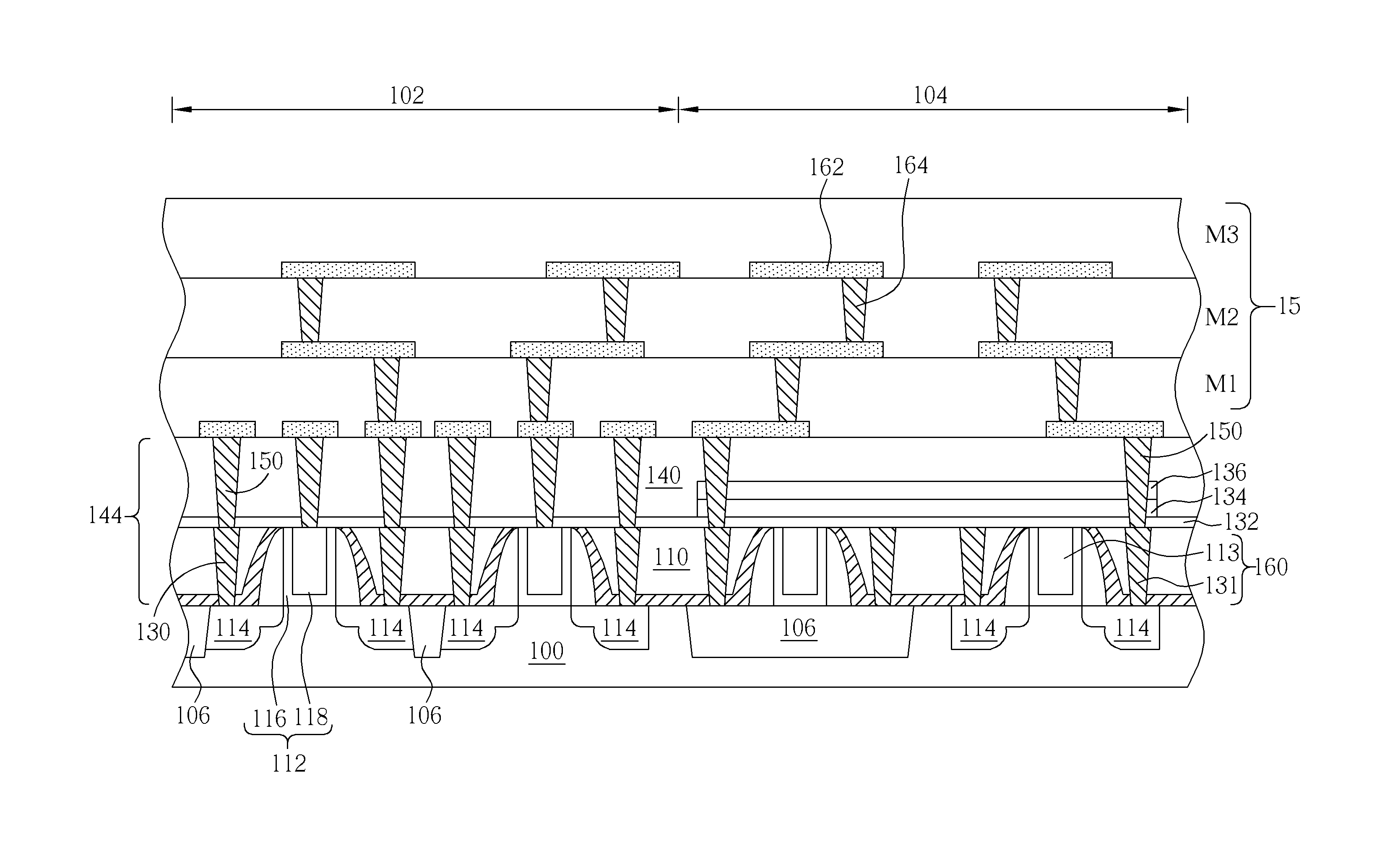
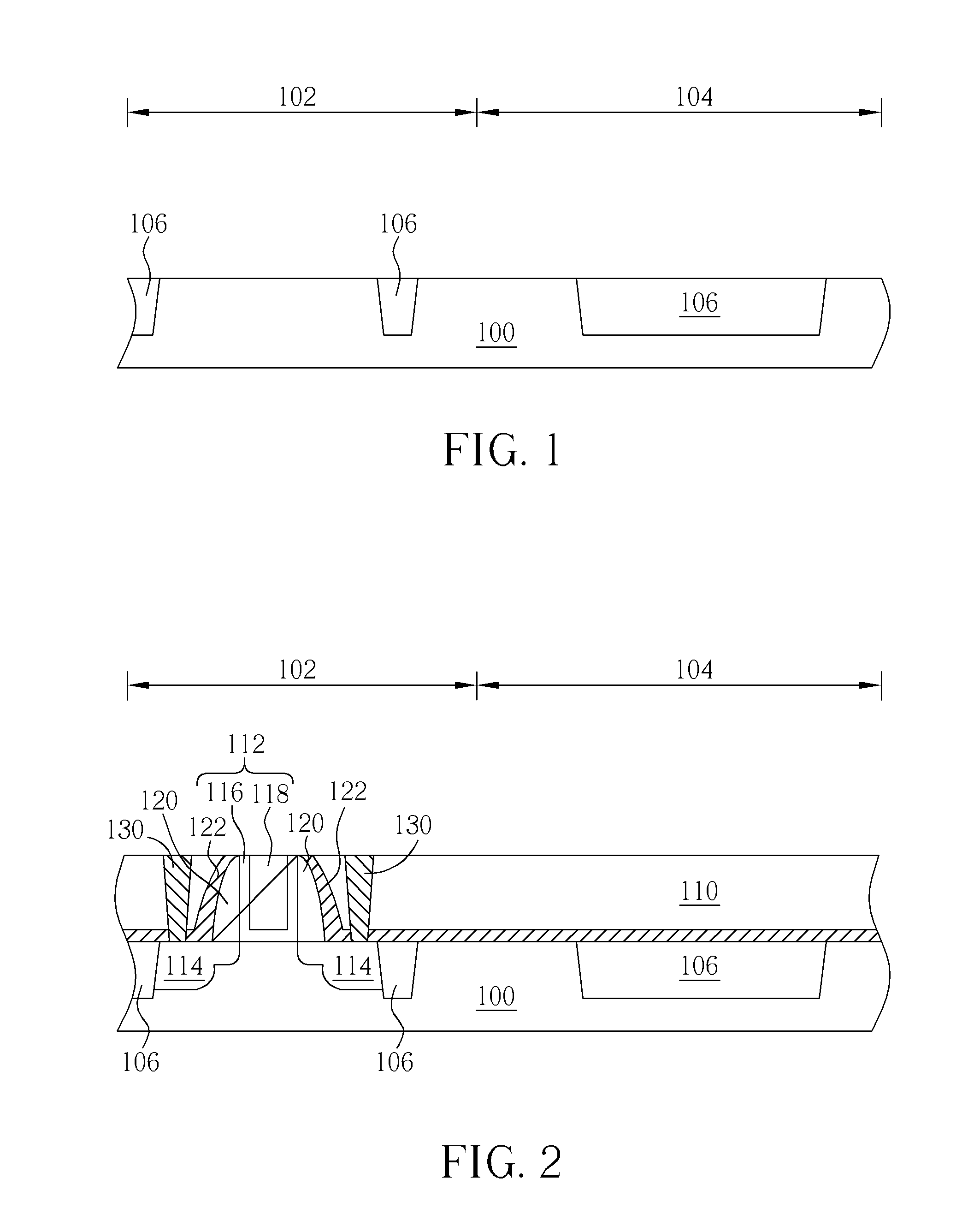
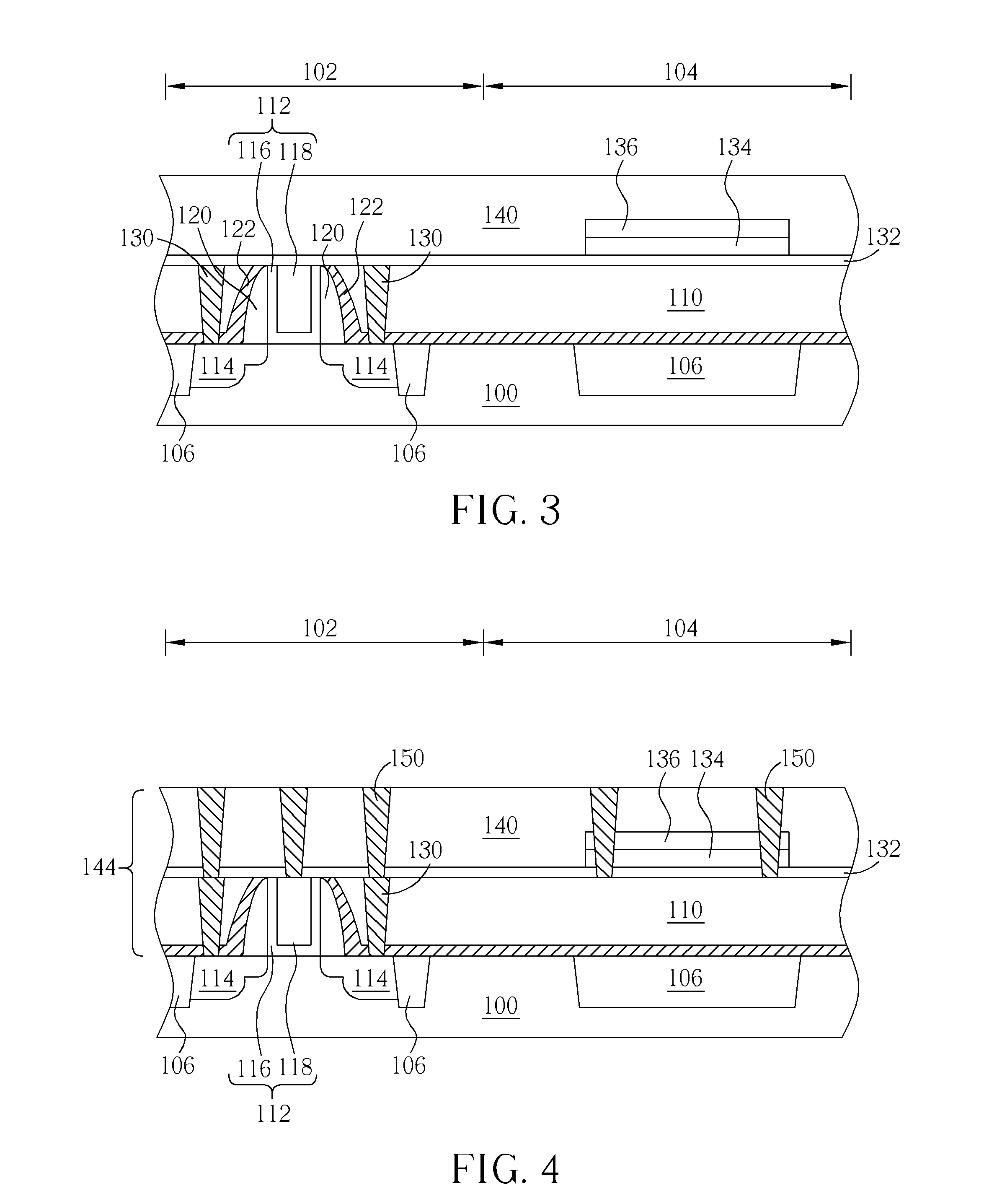
[0018]To provide a better understanding of the present invention to users skilled in the technology of the present invention, preferred embodiments are detailed as follows. The preferred embodiments of the present invention are illustrated in the accompanying drawings with numbered elements to clarify the contents and effects to be achieved.

[0019]Please refer to FIG. 1-5, FIGS. 1-5 are schematic diagrams illustrating a thin film resistor structure according to the first preferred embodiment of the present invention. Please note that the figures are only for illustration and may not be to scale. The scale may be further modified according to different design considerations. At first, as shown in FIG. 1, a substrate 100 is provided, a semiconductor region 102 and a resistor region 104 are on the substrate 100, and a plurality of STI (shallow trench isolation) 106 is then formed on the substrate 100 within the semiconductor region 102 and the resistor region 104. The substrate 100 may ...


PUM


Abstract

A thin film resistor structure includes a substrate, a flat bottom ILD (inter layer dielectric) disposed on the substrate, a plurality of first contacts disposed in the bottom ILD, and each top surface of the first contacts is on the same level as a top surface of the bottom ILD; a flat top ILD disposed on the bottom ILD, a plurality of second contacts disposed in the top ILD, and each top surface of the second contacts is on the same level as a top surface of the top ILD, and a thin film resistor disposed between the bottom ILD and the top ILD.

Description

BACKGROUND OF THE INVENTION[0001]1. Field of the Invention[0002]The present invention relates to a thin film resistor structure, and more particularly, to a thin film resistor structure integrated with a metal gate structure.[0003]2. Description of the Prior Art[0004]In the field of semiconductor fabrication, polysilicon material has been conventionally used to form the gates of metal-Oxide-Semiconductor Field-Effect (MOSFET) transistors. However, polysilicon materials have some drawbacks: the resistance of a polysilicon gate is higher than most of any metal materials, and the conductivity rate of the polysilicon gate is therefore lower than metal wires. In order to compensate for this disadvantage, the polysilicon gate usually undergoes a silicide process to simultaneously reduce the contact resistance and the parasitic resistance (Rn), so that the conductivity rate of the polysilicon gate is improved to an acceptable range.[0005]It is worth noting that the polysilicon is used not ...

Claims


Application Information

Patent Timeline
IPC IPC(8): H01L29/02
CPCH01L29/7833H01L23/5228H01L2924/0002H01L2924/00
Inventor WEI, MING-TETSAO, PO-CHAOTSAI, CHEN-HUACHEN, CHIEN-YANGLIANG, CHIA-JUICHEN, MING-TSUNG
Owner UNITED MICROELECTRONICS CORP
Why Eureka
Try Eureka