

Wiring structure, thin film transistor array substrate including the same, and display device
a technology of thin film transistors and array substrates, applied in semiconductor devices, semiconductor/solid-state device details, electrical apparatus, etc., can solve the problems of reducing the manufacture yield reducing the reliability of tft array substrates, so as to prevent the occurrence of film floating and facilitate electrical connectivity
- Summary
- Abstract
- Description
- Claims
- Application Information
AI Technical Summary
Benefits of technology
Problems solved by technology
Method used
Image

Examples
first preferred embodiment
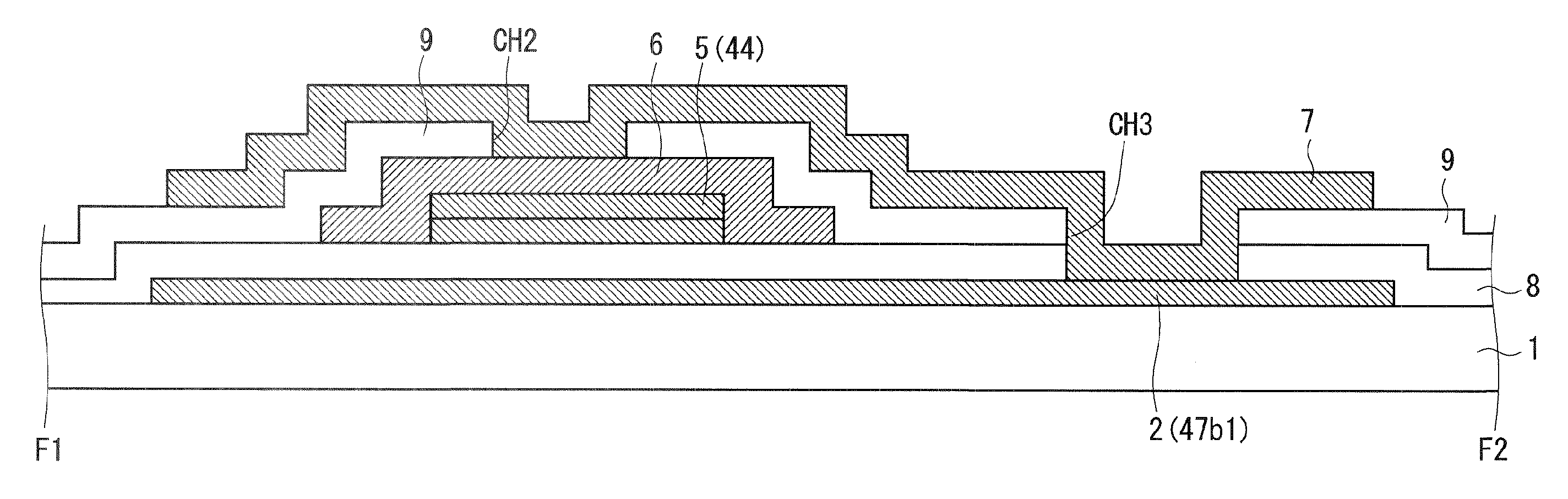
[0032]First, there is shown a configuration example of a liquid crystal display device capable of implementing a wiring structure according to the present invention. FIG. 1 is a plan view showing a TFT array substrate 100 of the liquid crystal display device according to a preferred embodiment of the present invention. As shown in FIG. 1, the TFT array substrate 100 includes pixels 50 serving as display units of an image, which are disposed on a substrate 1 in the form of an array (matrix). Each pixel 50 is provided with a TFT 51 serving as a switching element that supplies a display voltage to a pixel electrode (not shown). A member configured by the substrate 1 equipped with the TFTs 51 is called the “TFT array substrate” because the TFTs 51 are arranged for the respective pixels 50 in the form of the array. The substrate 1 includes a glass substrate or a semiconductor substrate.
[0033]The TFT array substrate 100 has an array region 41 (region inside a rectangle shown by a dotted l...
second preferred embodiment
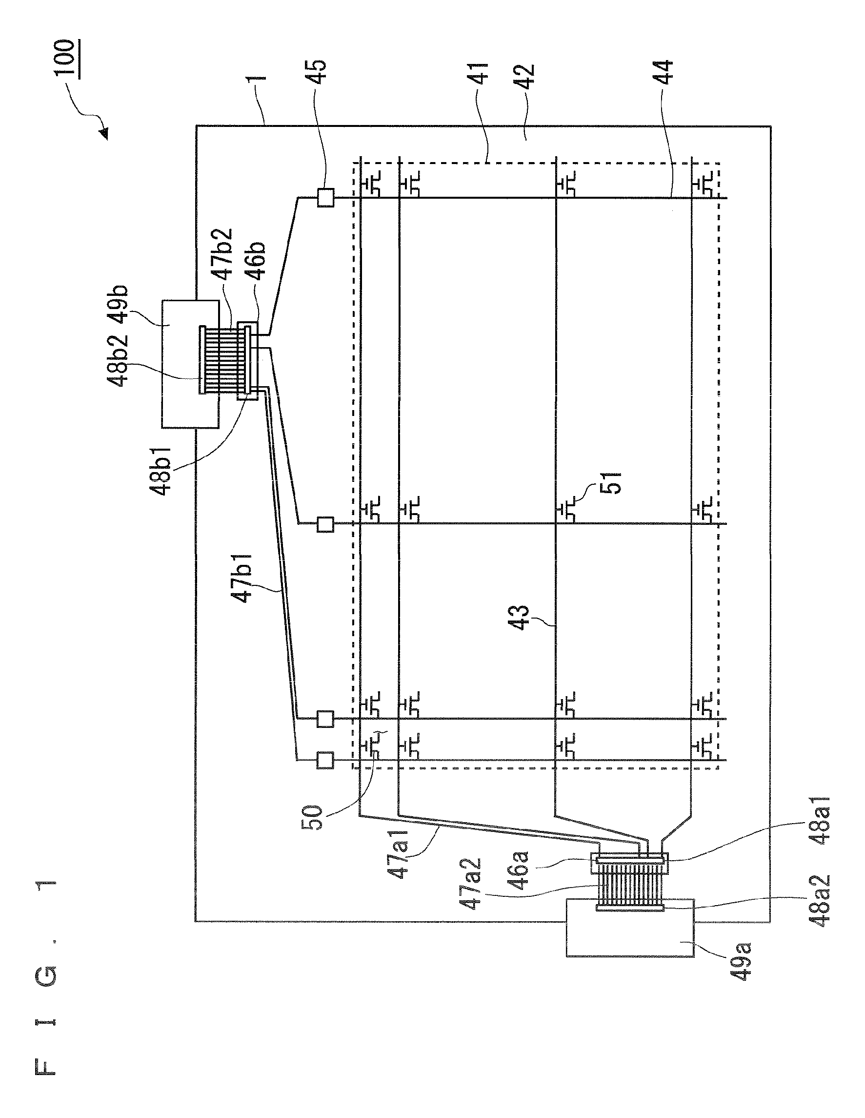
[0126]FIG. 14 is a plan view of the wiring conversion part 45 provided on the TFT array substrate 100 according to a second preferred embodiment. Sectional views taken along line B1-B2 and taken along line C1-C2 in FIG. 14 are the same as those in FIG. 6 and FIG. 7, so that descriptions thereof are omitted here.
[0127]Similarly to the first preferred embodiment, in the wiring conversion part 45 in the second preferred embodiment, the first transparent conductive film 6 covers the end surface of the first conductive film 5, and an angle formed at the corner part in the portion of the first transparent conductive film 6 making direct contact with the first insulating film 8 is larger than 90 degrees and smaller than 270 degrees. In the wiring conversion part 45 shown in FIG. 14, the first transparent conductive film 6 has eight corner parts P21, P22, P23, P24, P25, P26, P27, and P28 in the portion making direct contact with the first insulating film 8, and angles θ21, θ22, θ23, θ24, θ2...
third preferred embodiment
[0132]FIG. 15 is a plan view of the wiring conversion part 45 provided on the TFT array substrate 100 according to a third preferred embodiment. Sectional views taken along line B1-B2 and taken along line C1-C2 in FIG. 15 are the same as those in FIG. 6 and FIG. 7, respectively, so that descriptions thereof are omitted here.
[0133]Similarly to the first preferred embodiment, in the wiring conversion part 45 in the third preferred embodiment, the first transparent conductive film 6 covers the end surface of the first conductive film 5. Furthermore, according to the present preferred embodiment, a corner part in the portion of the first transparent conductive film 6 which makes direct contact with the first insulating film 8 has an arc shape. According to an example in FIG. 15, the first transparent conductive film 6 is rectangular in shape having arc-shaped round corner parts. In the wiring conversion part 45 shown in FIG. 15, the first transparent conductive film 6 has four corner pa...
PUM
| Property | Measurement | Unit |
|---|---|---|
| angle | aaaaa | aaaaa |
| structure | aaaaa | aaaaa |
| transparent conductive | aaaaa | aaaaa |
Abstract
Description
Claims
Application Information