
Method of fabricating a package substrate

a technology of packaging substrate and substrate plate, which is applied in the direction of semiconductor devices, semiconductor/solid-state device details, electrical equipment, etc., can solve the problems of deteriorating bump reliability, high hardness of copper post, and easy oxidation of copper post, so as to improve the composition and formation of post terminals

Inactive Publication Date: 2013-09-12
SAMSUNG ELECTRO MECHANICS CO LTD
View PDF6 Cites 1 Cited by
  • Summary
  • Abstract
  • Description
  • Claims
  • Application Information

AI Technical Summary

Benefits of technology

The solution effectively controls warpage and prevents undesired plating, maintaining reliability by using a ductile alloy post terminal and a solder bump with a lower melting point, enhancing the structural integrity and reducing the risk of cracking and separation.

Problems solved by technology

The change of the flip chip package under the above trend causes a problem of deteriorating bump reliability, and accordingly the improvement thereof is required.
However, such a copper post has some problems.
The copper post is easily oxidized and has a great degree of hardness, so it is susceptible to cracking or short circuiting when warpage between the substrate and the chip occurs.
However, when a post is formed of such a metallic alloy, separation between a metal seed layer and a dry film has occurred, and accordingly, an undesired plating of an insulating layer may be performed or a desired plating of a pad may not be performed.

Method used


Image

  • Method of fabricating a package substrate
  • Method of fabricating a package substrate
  • Method of fabricating a package substrate

Examples


Embodiment Construction

[0034]Exemplary embodiments of the present invention will now be described in detail with reference to the accompanying drawings.

[0035]The invention may, however, be embodied in many different forms and should not be construed as being limited to the embodiments set forth herein. Rather, these embodiments are provided so that this disclosure will be thorough and complete, and will fully convey the scope of the invention to those skilled in the art. In the drawings, the shapes and dimensions may be exaggerated for clarity, and the same reference numerals will be used throughout to designate the same or like components.

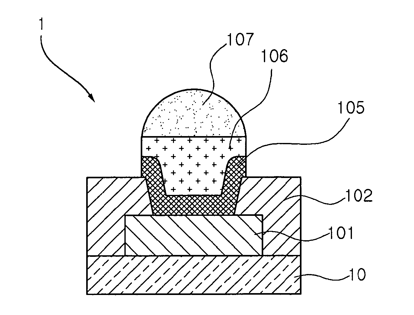
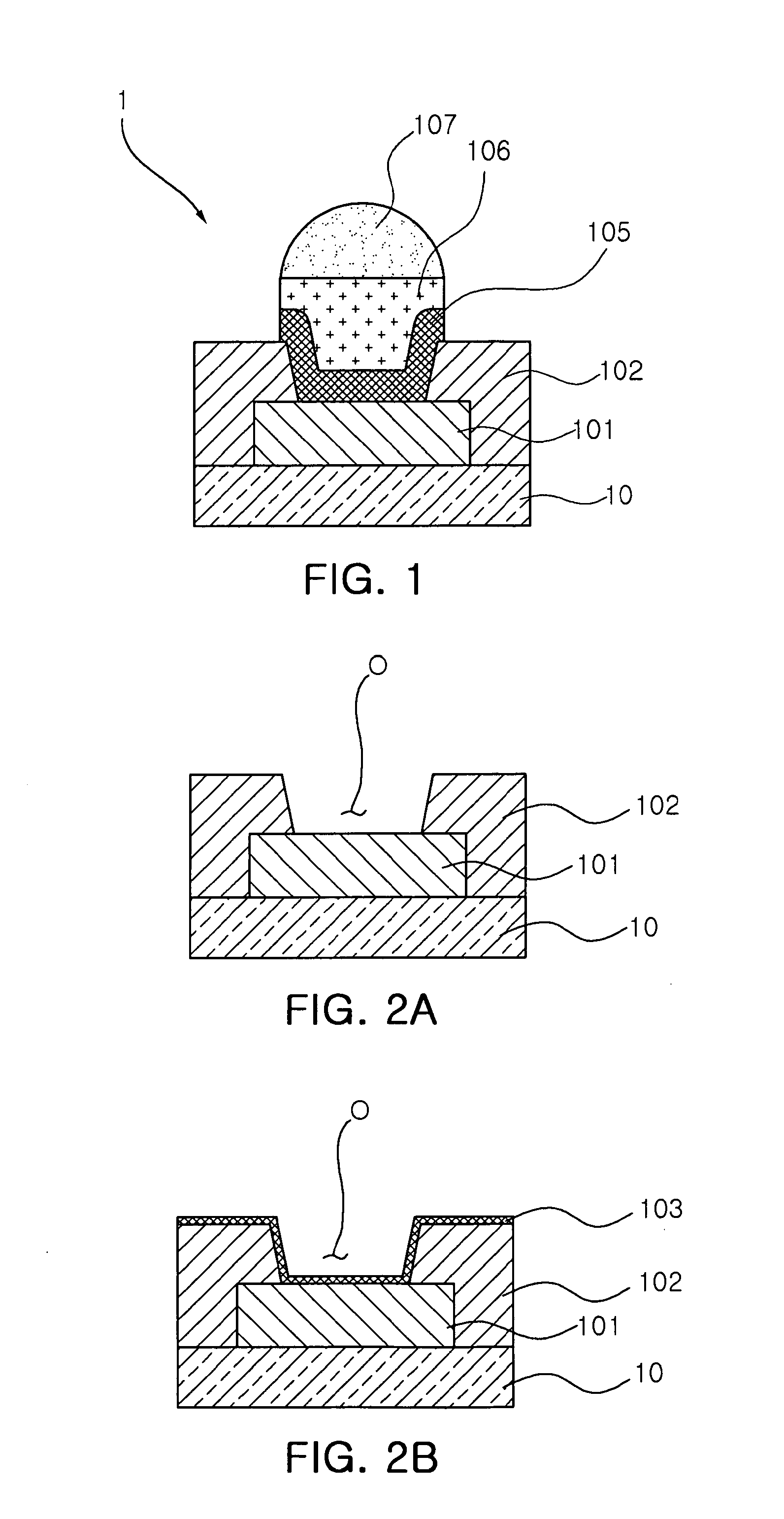
[0036]Hereinafter, a package substrate according to an exemplary embodiment of the present invention will be described with reference to FIG. 1.

[0037]FIG. 1 is a schematic cross-sectional view illustrating a package substrate according to an exemplary embodiment of the present invention.

[0038]A package substrate 1 according to this embodiment includes a substrate 10 hav...


PUM


Abstract

A method of fabricating a package substrate including preparing a substrate having at least one conductive pad, forming an insulating layer having an opening to expose the conductive pad on the substrate, forming a separation barrier layer on the conductive pad inside the opening to be higher than the upper surface of the insulating layer along the side walls thereof, forming a post terminal on the separation barrier layer, and forming a solder bump on the post terminal.

Description

CROSS-REFERENCE TO RELATED APPLICATIONS[0001]This application is a divisional application of U.S. application Ser. No. 12 / 926,314, filed Nov. 9, 2010, now pending, which in turn claims the priority of Korean Patent Application No. 10-2009-0121098, filed on Dec. 8, 2009, in the Korean Intellectual Property Office, the disclosure of which is incorporated herein by reference.BACKGROUND[0002]1. Field[0003]The present invention relates to a package substrate and a method of fabricating the same, and more particularly, to a package substrate capable of controlling the degree of warpage thereof by improving the composition and formation of a post terminal and a method of fabricating the same.[0004]2. Description of the Related Art[0005]A flip chip package has solder bumps formed on a chip and a substrate in contact with each other.[0006]With an increase in data processing capacity and the trend for lighter, thinner, shorter and smaller semiconductors, a flip chip package used for high-spee...

Claims


Application Information

Patent Timeline
Patent Type & Authority Applications(United States)
IPC IPC(8): H01L21/48
CPCH01L23/485H01L24/11H01L21/4853H01L21/441H01L24/03H01L24/05H01L24/13H01L2224/0346H01L2224/11849H01L2224/13082H01L2224/05572H01L2224/0347H01L2224/1147H01L23/48
Inventor LEE, DONG GYULEE, DAE YOUNGCHUNG, TAE JOONMUN, SEON JAECHOI, JIN WON
Owner SAMSUNG ELECTRO MECHANICS CO LTD
Learn More