Eureka AIR delivers breakthrough ideas for toughest innovation challenges, trusted by R&D personnel around the world.

Scan flip-flop, method thereof and devices having the same

Active Publication Date: 2013-09-19
SAMSUNG ELECTRONICS CO LTD
View PDF3 Cites 14 Cited by
  • Summary
  • Abstract
  • Description
  • Claims
  • Application Information

AI Technical Summary

Benefits of technology

The patent text describes a scan flip-flop that can perform both a normal operation and a scan operation. The flip-flop uses an intermediate node voltage to synchronize the data input and the scan input. The flip-flop includes a first circuit that determines the intermediate node voltage based on the clock signal and the data input during the normal operation, and a second circuit that determines the data based on the clock signal, the intermediate node voltage, and the data input during the scan operation. The flip-flop also includes a latch that latches the data based on the clock signal. The technical effect of this invention is to provide a more efficient and flexible method for processing data during a scan operation.

Problems solved by technology

However, using the master-slave flip-flop in the high-speed operating chip reaches a limit due to data-to-output latency.
However, a yield of a chip using the pulse flip-flop or the semi-dynamic flip-flop is not good because of unstable characteristics of a pulse, and it is not easy to integrate the pulse-flip-flop or the semi-dynamic flip-flop on the chip because of a long hold time.

Method used


Image

  • Scan flip-flop, method thereof and devices having the same
  • Scan flip-flop, method thereof and devices having the same
  • Scan flip-flop, method thereof and devices having the same

Examples


Embodiment Construction

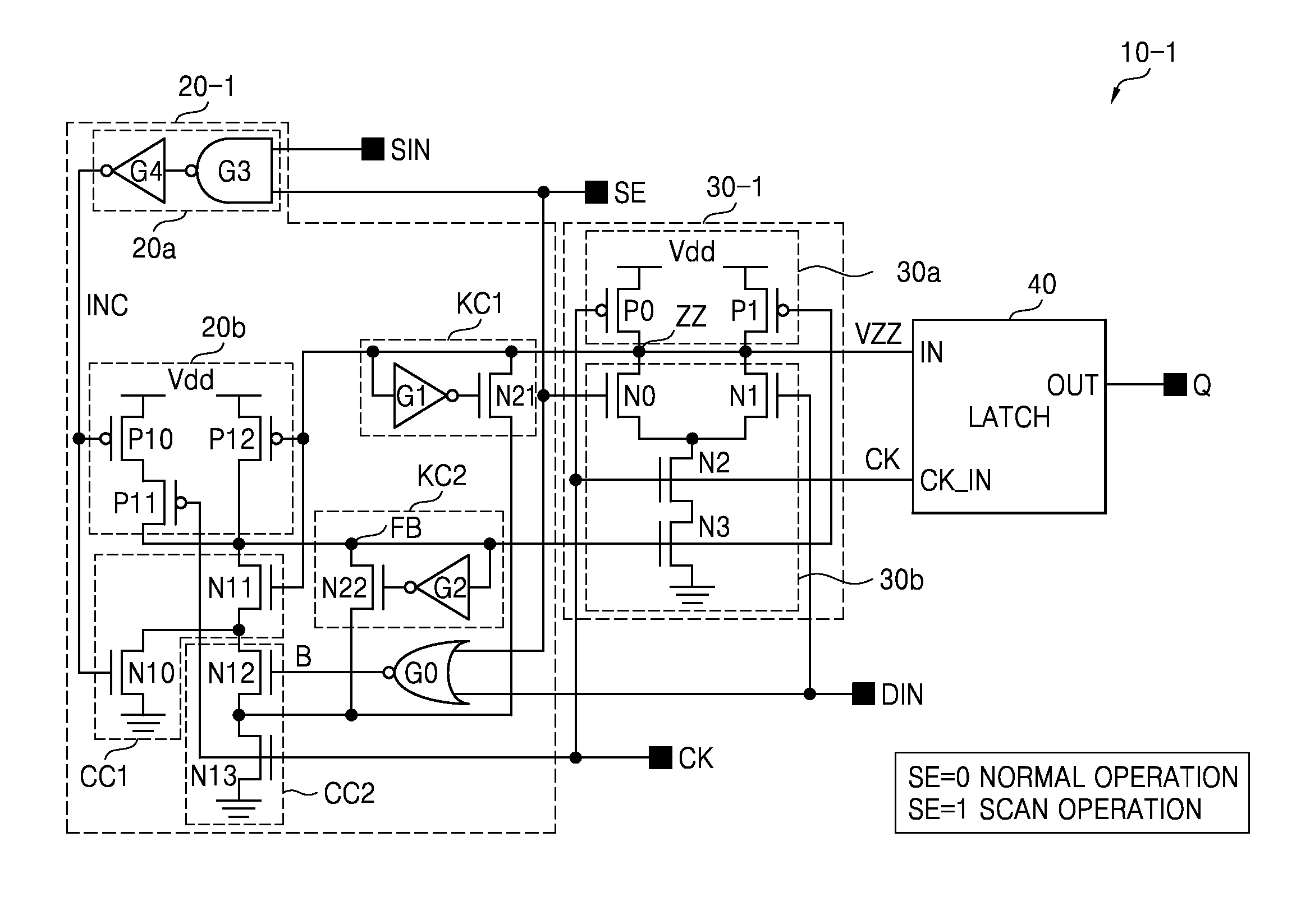
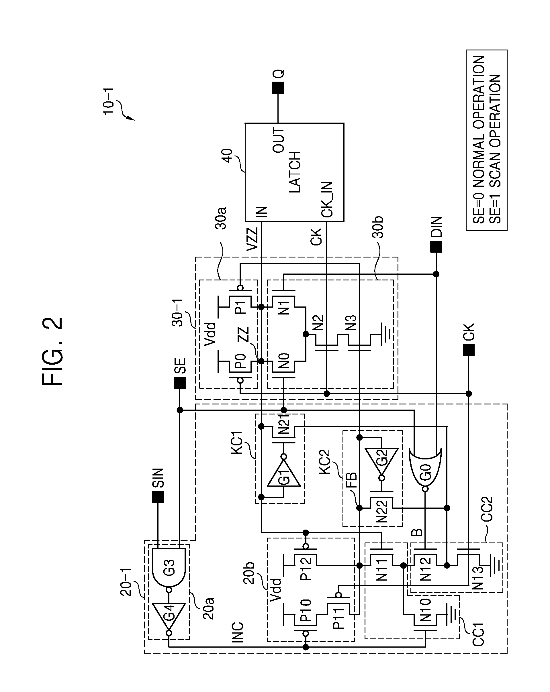
[0039]A scan input of the inventive concepts means a signal generated according to a logical combination of a scan data SIN and a scan enable signal SE, or the scan data SIN itself.

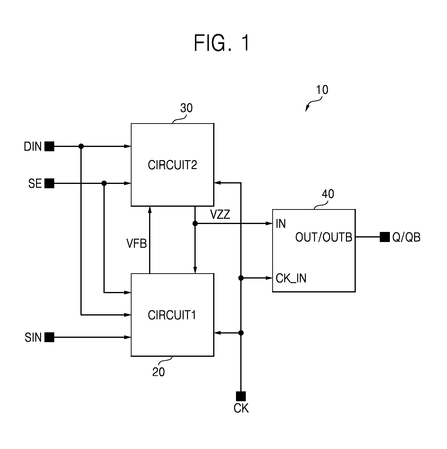
[0040]FIG. 1 is a schematic block diagram of a scan flip-flop according to an example embodiment. Referring to FIG. 1, a scan flip-flop 10 may include a first circuit 20, a second circuit 30, and a latch 40.

[0041]The scan flip-flop 10 may perform selectively a normal operation, e.g., latching a data input DIN, and a scan operation, e.g., latching a scan data SIN, based on a level of a scan enable signal SE. According to an exemplary embodiment, the data input DIN may be a parallel data including one-bit or more. For example, when the level of the scan enable signal SE is a first level, e.g., a low level or a logic 0, the scan flip-flop 10 may perform a normal operation. In addition, when the level of the scan enable signal SE is a second level, e.g., a high level or a logic 1, the scan flip-flop 10 may pe...


PUM


Abstract

A scan flip-flop, which performs a normal operation latching a data input and a scan operation latching a scan input, includes a first circuit, a second circuit and a latch. The first circuit determines a voltage of an intermediate node based on a clock signal, one of the data input and the scan input, and data of a latch input node. The second circuit determines the data based on the clock signal, the voltage of the intermediate node and the data input during the normal operation, and determines the data based on the clock signal and the voltage of the intermediate node during the scan operation. The latch latches the data based on the clock signal.

Description

CROSS-REFERENCE TO RELATED APPLICATION[0001]This application claims priority under 35 U.S.C. §119(a) from Korean Patent Application No. 10-2012-0027387 filed on Mar. 16, 2012, the disclosure of which is hereby incorporated by reference in its entirety.BACKGROUND[0002]1. Field[0003]Apparatuses and methods consistent with exemplary embodiments of the inventive concept relate to a scan flip-flop, and more particularly, to a high-speed low-power scan flip-flop, an operating method thereof and data processing devices having the same.[0004]2. Description of the Related Art[0005]To design a high speed operation chip, designing a high speed flip-flop may be required. A related-art master-slave flip-flop is widely used due to its small size and low power consumption. However, using the master-slave flip-flop in the high-speed operating chip reaches a limit due to data-to-output latency. To improve the limit of the master-slave flip-flop, a pulse flip-flop or a semi-dynamic flip-flop is devel...

Claims


Application Information

Patent Timeline
IPC IPC(8): H03K3/037H03K3/00
CPCH03K3/356139G01R31/318541H03K3/286
Inventor KIM, MIN SU
Owner SAMSUNG ELECTRONICS CO LTD
Why Eureka
Eureka Blog
Learn More