Method of manufacturing semiconductor element

a manufacturing method and semiconductor technology, applied in semiconductor devices, semiconductor/solid-state device details, electrical devices, etc., can solve the problems of destroying the wafer during subsequent laser liftoff (llo) of the growth substrate, affecting the efficiency of heat dissipation, and affecting the production efficiency of semiconductor elements, etc., to achieve excellent productivity, good yield and reliability, and less voids

Active Publication Date: 2013-09-19
STANLEY ELECTRIC CO LTD
View PDF6 Cites 2 Cited by
  • Summary
  • Abstract
  • Description
  • Claims
  • Application Information

AI Technical Summary

Benefits of technology

[0007]One object of this invention is to provide a method of manufacturing a semiconductor element, such as LED, with excellent productivity, manufacturing yields and reliability. The semiconductor element has a thermally conductive supporting substrate. In bonding a semiconductor wafer to the supporting substrate, the present invention achieves uniform joining of the semiconductor wafer and the supporting substrate at low temperature and with few voids. Also, the invention prevents warping and / or destruction of the semiconductor wafer and supporting substrate due to the bonding treatment and / or subsequent growth substrate removal.

Problems solved by technology

In addition, the efficiency of heat dissipation is poor because of the low thermal conductivity of the growth substrate.
Further, if there are irregularities in the temperature over the wafer surface, irregularities occur in the melting or softening, and large voids measuring several microns or more occur in the bond portion.
Moreover, because treatment must be performed at high temperature, warping of the wafer during bonding due to a difference in the thermal expansion coefficients of the semiconductor layer and the thermally conductive supporting substrate may occur, and destruction of the wafer during subsequent laser liftoff (LLO) of the growth substrate may occur.
These result in reduced manufacturing yields and reduced reliability of light-emitting elements manufactured by eutectic bonding.

Method used


Image

  • Method of manufacturing semiconductor element
  • Method of manufacturing semiconductor element
  • Method of manufacturing semiconductor element

Examples


embodiment 1

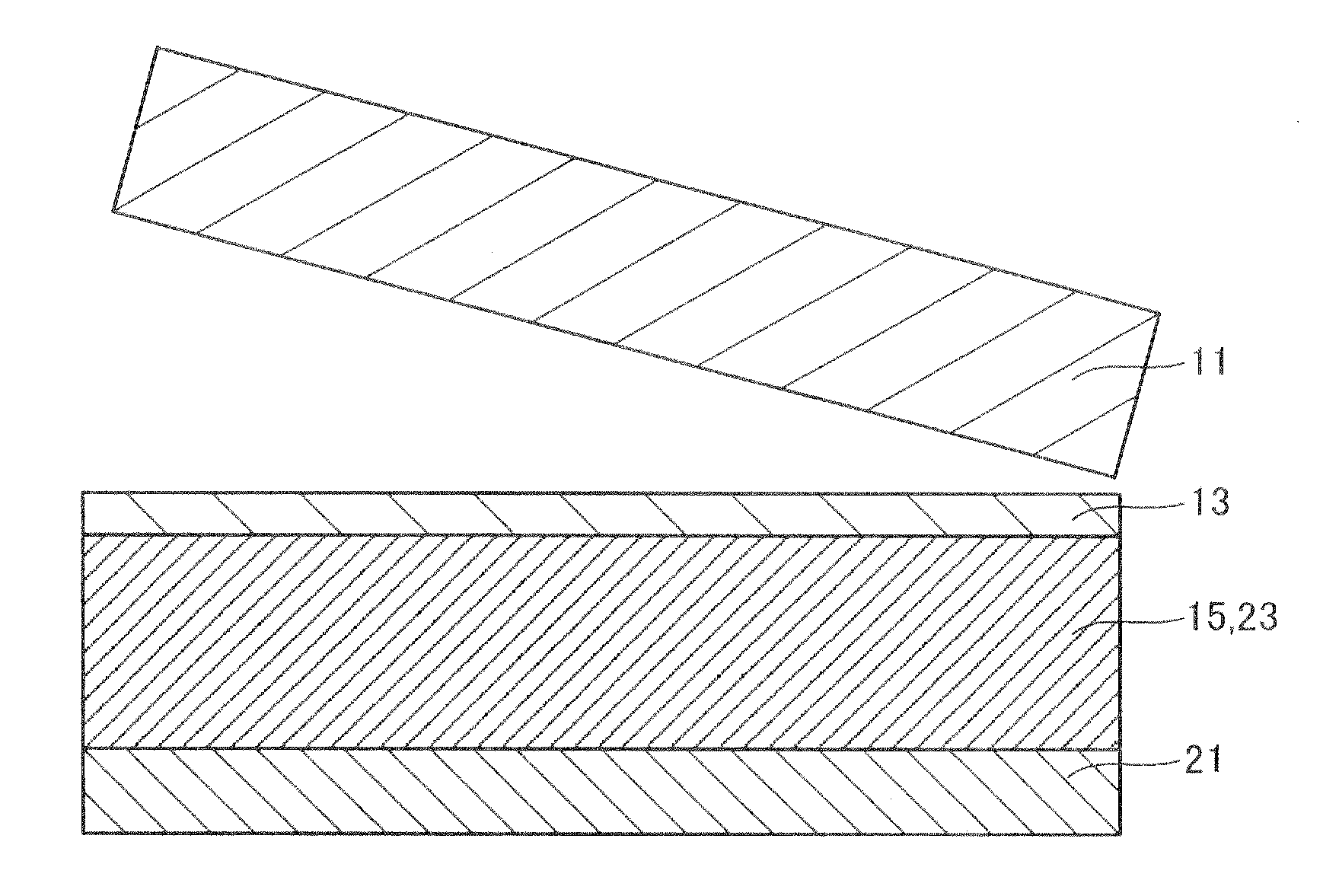
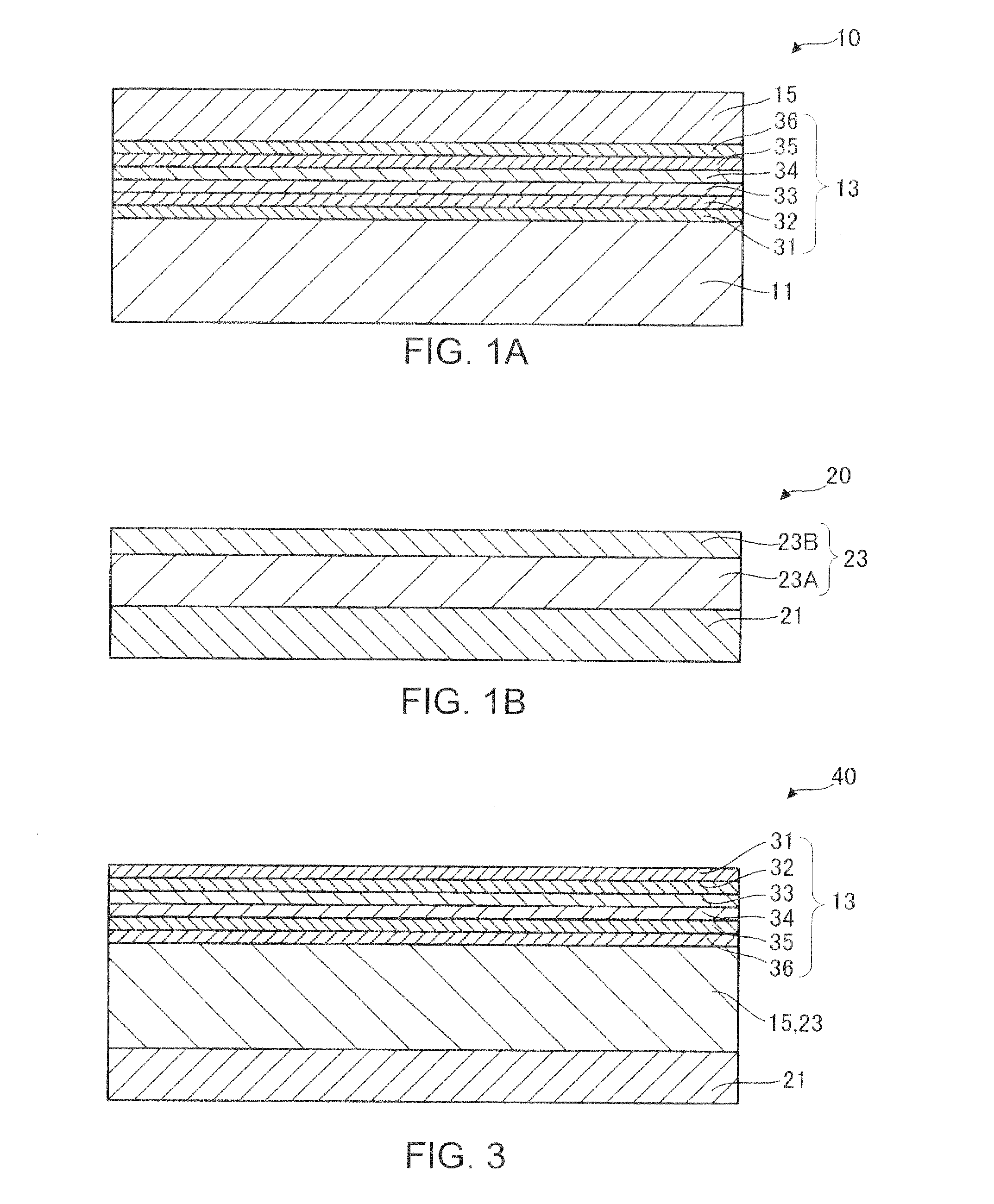
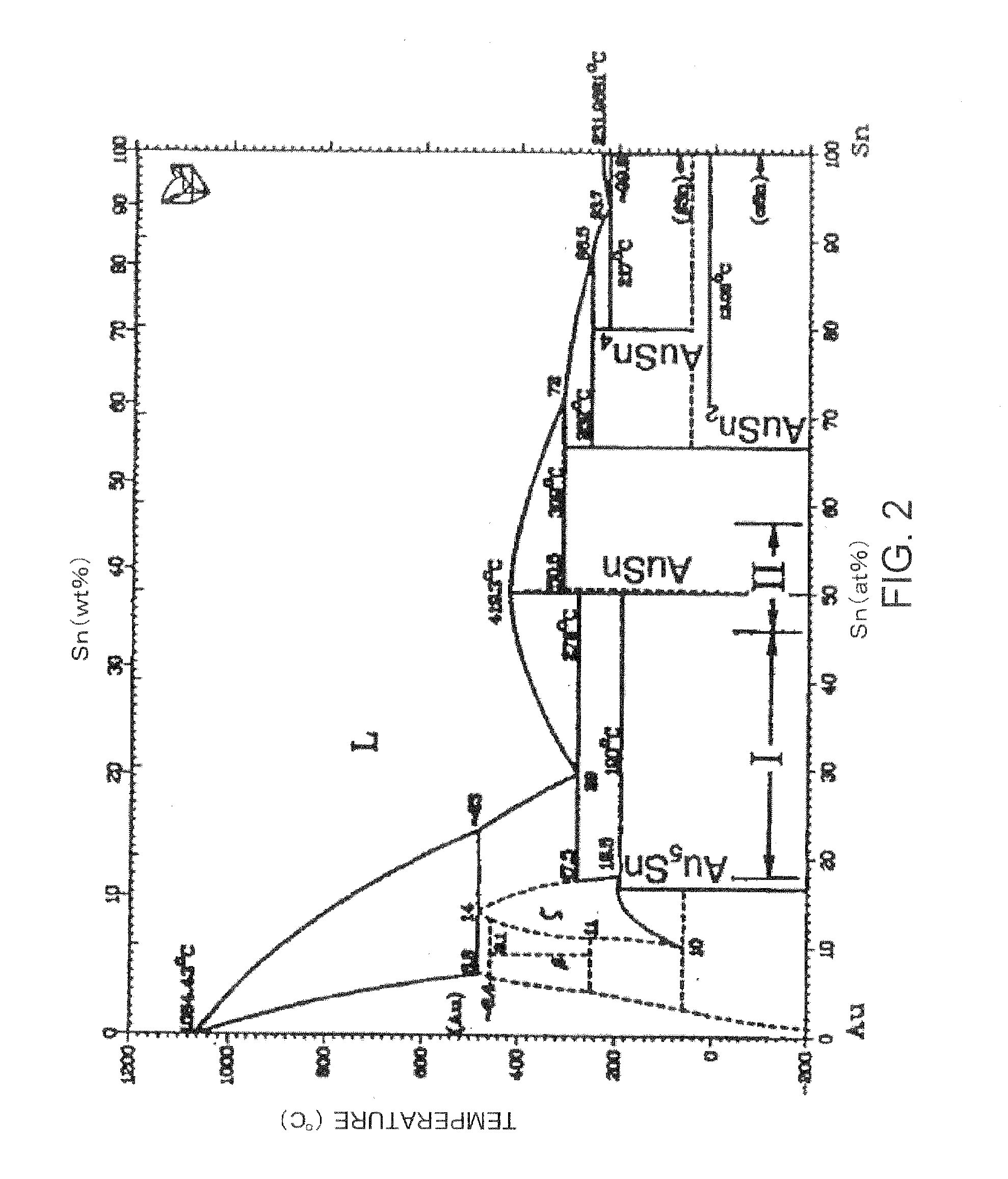
[0019]A method of manufacturing a light-emitting element according to Embodiment 1 of the invention is described below, referring to FIG. 1A, FIG. 1B, FIG. 2 and FIG. 3. FIG. 1A shows a semiconductor water 10 that is to be bonded to a supporting structure20 shown in FIG. 1B by the method of manufacturing the light-emitting element 40 of Embodiment 1. FIG. 3 illustrates a resulting light-emitting element 40. FIG. 2 is an Au—Sn alloy state diagram.

[0020]As shown in FIG. 1A, the semiconductor wafer 10 includes a growth substrate 11, an element structure layer (device layer) 13 grown on the growth substrate 11, and a first bonding layer 15 formed on the upper face of the element structure layer 13.

[0021]Firstly, the growth method of the element structure layer 13 is described. For example, an MOCVD method is used in epitaxial growth, on the (001) face of a sapphire substrate 11 of thickness 430 μm and diameter 2 inches, with the growth temperature between approximately 500° C. and 1100°...


PUM

PropertyMeasurementUnit
temperatureaaaaaaaaaa
thicknessaaaaaaaaaa

Abstract

A method of manufacturing a semiconductor element includes forming an element structure layer having a semiconductor layer, on a first substrate. The method also includes forming a first bonding layer on the element structure layer. The method also includes forming a second bonding layer on a second substrate. The method also includes performing heating pressure-bonding on the first and second bonding layers, with the first and second bonding layers facing each other. One of the first bonding layer and the second bonding layer is an AU layer, and the other is an AuSn layer. The AuSn layer has a surface layer having an Sn content of between 85 wt % (inclusive) and 95 wt % (inclusive).

Description

BACKGROUND OF THE INVENTION[0001]1. Field of the Invention[0002]The present invention relates to a method of manufacturing a semiconductor element, and in particular a method of manufacturing a light-emitting diode (LED).[0003]2. Description of the Related Art[0004]Light-emitting devices equipped with LED elements are used in, for example, illumination, backlighting and industrial equipment. Efforts are expended to increase the brightness of light-emitting elements in such light-emitting devices. LED elements are manufactured by using, for example, a metal-organic chemical vapor deposition (MOCVD) method to deposit a semiconductor layer of AlGaInP or GaN by epitaxial growth on a GaAs substrate, sapphire substrate or other suitable growth substrates. In an LED element manufactured in this way, light emitted from the light emission layer is absorbed in the growth substrate so that the efficiency of light extraction is reduced. In addition, the efficiency of heat dissipation is poor be...

Claims


Application Information

Patent Timeline
Patent Type & Authority Applications(United States)
IPC IPC(8): H01L33/60
CPCH01L24/29H01L33/0079H01L24/83H01L2224/29111H01L2224/29144H01L2224/83193H01L2224/83203H01L2224/83805H01L2924/013H01L24/32H01L33/405H01L33/641H01L2924/12041H01L2933/0075H01L23/3735H01L33/60H01L2924/01322H01L2924/0105H01L2924/01079H01L2924/00H01L2924/12042H01L33/0093
Inventor CHINONE, TAKAKOMIYACHI, MAMORUSAITO, TATSUMAAKAGI, TAKANOBU
Owner STANLEY ELECTRIC CO LTD
Why Eureka
Try Eureka