Semiconductor device

a semiconductor and device technology, applied in the field of semiconductor devices, to achieve the effect of safe semiconductor devices and without reducing efficiency

Inactive Publication Date: 2013-09-26
ABLIC INC
View PDF16 Cites 8 Cited by
  • Summary
  • Abstract
  • Description
  • Claims
  • Application Information

AI Technical Summary

Benefits of technology

[0013]The semiconductor device having an overheat and overcurrent protective function according to the present invention can set arbitrary overcurrent protection characteristics in accordance with the allowable power dissipation characteristics of the semiconductor device, and thus, a safe semiconductor device can be provided without reducing the efficiency.

Problems solved by technology

However, in the conventional technology, the safe operating area of a semiconductor device does not conform to the actual characteristics of the allowable power dissipation of the semiconductor device, and, even within the safe operating area, there is an area in which the protective circuits operate and thus the semiconductor device cannot be used.

Method used


Image

  • Semiconductor device
  • Semiconductor device
  • Semiconductor device

Examples


first embodiment

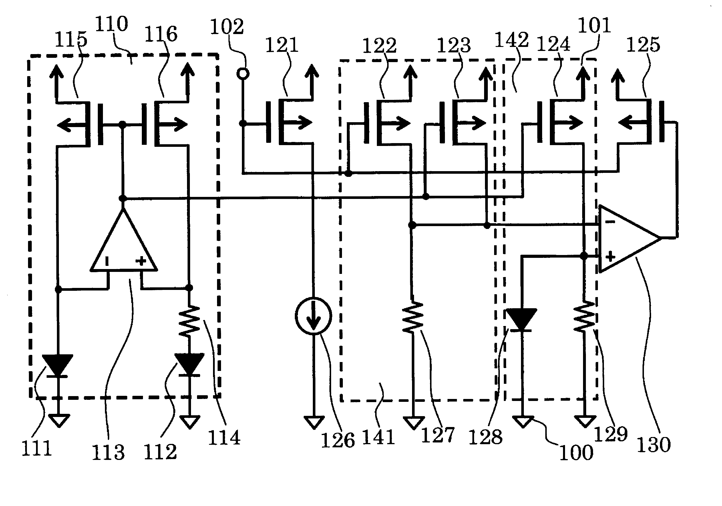
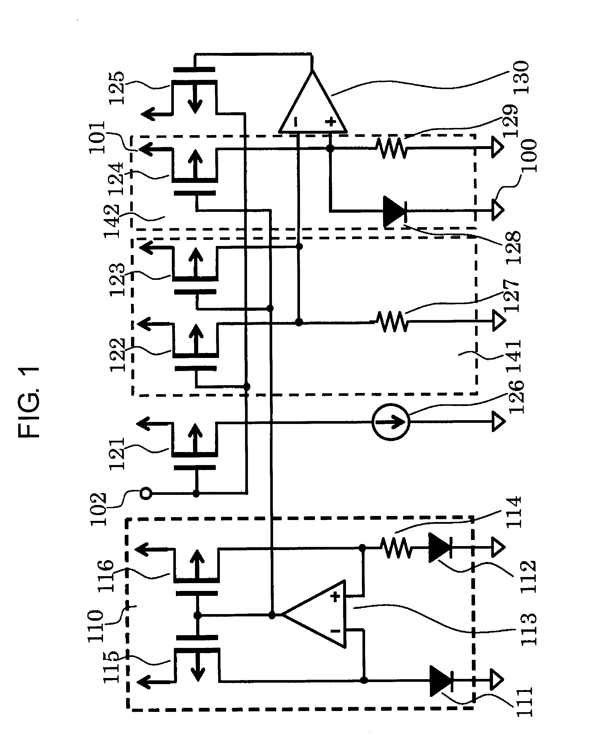
[0020]FIG. 1 is a circuit diagram of a semiconductor device according to a first embodiment of the present invention.

[0021]The semiconductor device of the first embodiment includes amplifiers 113 and 130, PMOS transistors 115, 116, 121, 122, 123, 124, and 125, a load current source 126, PN junction elements 111, 112, and 128, resistors 114, 127, and 129, a power supply terminal 101, a control terminal 102, and a ground terminal 100. The PMOS transistors 115 and 116, the amplifier 113, the PN junction elements 111 and 112, and the resistor 114 form a reference current circuit 110. The PMOS transistors 122 and 123 and the resistor 127 form a sense voltage generating circuit 141. The PMOS transistor 124, the PN junction element 128, and the resistor 129 form a reference voltage circuit 142.

[0022]Next, connection in the semiconductor device of the first embodiment is described. An inverting input terminal of the amplifier 113 is connected to a node between a drain of the PMOS transistor...

second embodiment

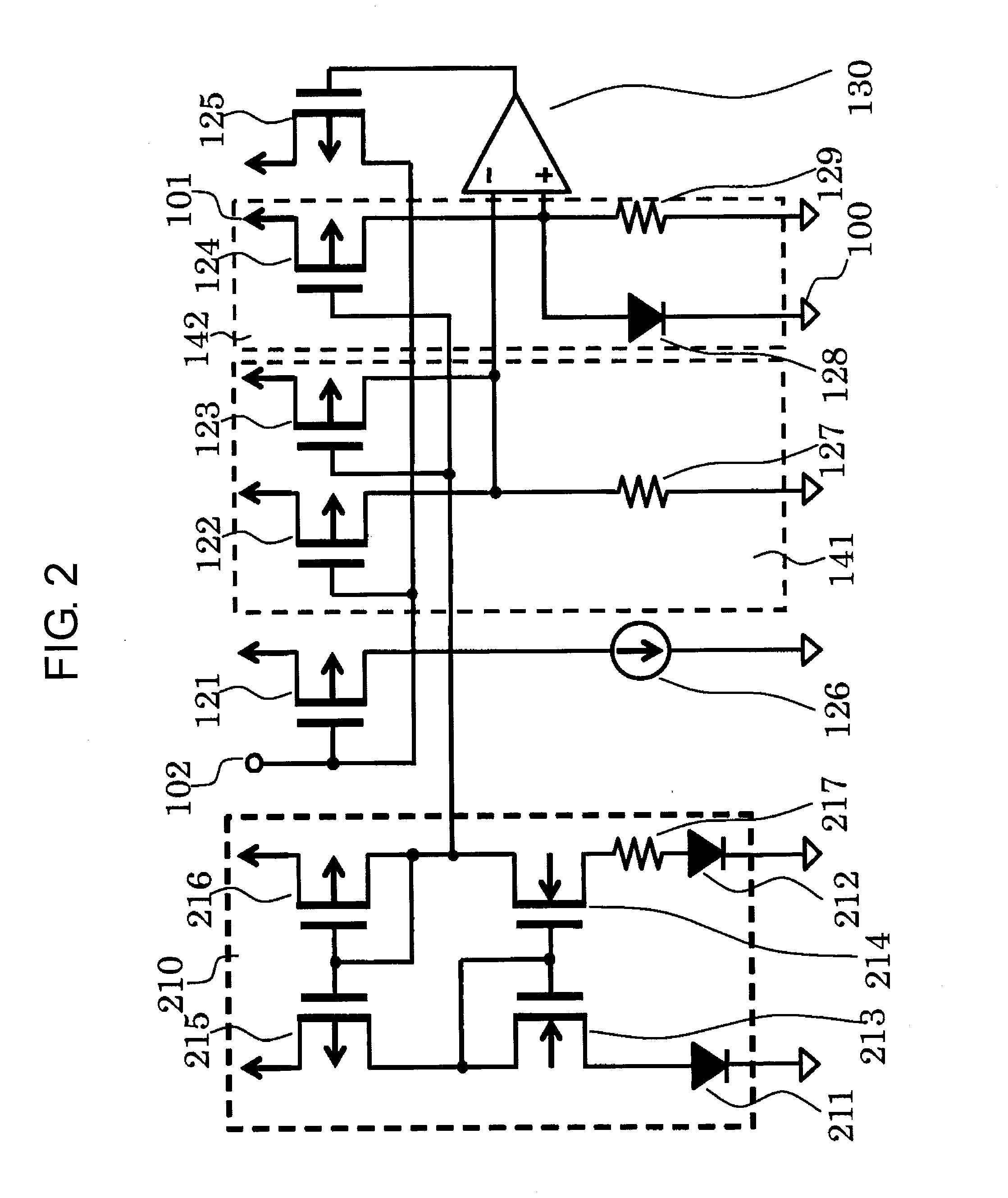
[0031]FIG. 2 is a circuit diagram of a semiconductor device according to a second embodiment of the present invention. The circuit is different from the circuit illustrated in FIG. 1 in the structure of the reference current circuit 110. In the semiconductor device of the second embodiment, PMOS transistors 215 and 216, NMOS transistors 213 and 214, PN junction elements 211 and 212, and a resistor 217 form a reference current circuit 210. Except for this point, the second embodiment is the same as the first embodiment.

[0032]Connection in the semiconductor device of the second embodiment is now described. A gate of the PMOS transistor 215 is connected to a gate and a drain of the PMOS transistor 216, a drain of the PMOS transistor 215 is connected to a gate and a drain of the NMOS transistor 213 and to a gate of the NMOS transistor 214, and a source of the PMOS transistor 215 is connected to the power supply terminal 101. A source of the PMOS transistor 216 is connected to the power ...


PUM


Abstract

The semiconductor device includes: a first transistor controlled by a control signal; a sense voltage generating circuit for sensing current flowing through the first transistor, mirroring current flowing through a reference current circuit, and summing the currents to generate voltage based on the summed currents; a reference voltage circuit for mirroring current flowing through the reference current circuit and generating reference voltage; an amplifier for comparing the voltage generated by the sense voltage generating circuit and the reference voltage; and a second transistor which has a gate connected to an output terminal of the amplifier and which can turn off the first transistor.

Description

RELATED APPLICATIONS[0001]This application claims priority under 35 U.S.C. §119 to Japanese Patent Application No. 2012-068024 filed on Mar. 23, 2012, the entire content of which is hereby incorporated by reference.BACKGROUND OF THE INVENTION[0002]1. Field of the Invention[0003]The present invention relates to a semiconductor device having an overheat and overcurrent protective function.[0004]2. Description of the Related Art[0005]A conventional semiconductor device is described with reference to FIG. 4 which is a circuit diagram illustrating the conventional semiconductor device.[0006]The conventional semiconductor device includes an overcurrent detection unit 304, a thermal shut down detection unit (hereinafter referred to as TSD detection unit) 309, NMOS transistors 301, 302, 306, and 307, resistors 303, 305, and 308, a ground terminal 100, and external terminals 321 and 322. The overcurrent detection unit 304, the resistor 303, and the NMOS transistor 306 form an overcurrent pro...

Claims


Application Information

Patent Timeline
Patent Type & Authority Applications(United States)
IPC IPC(8): H03K17/081H03K17/14
CPCH03K17/081H03K2017/0806H03K17/0822H03K17/145H03K17/08H03K17/14H01L27/04
Inventor SAKAGUCHI, KAORU
Owner ABLIC INC
Why Eureka
Try Eureka