Semiconductor package, package structure and fabrication method thereof

a technology of semiconductor chips and packaging, applied in the direction of semiconductor/solid-state device details, electrical equipment, semiconductor devices, etc., can solve the problems of increasing fabrication time and cost, limited number and size of semiconductor chips, etc., and achieve the effect of increasing product competitiveness and saving fabrication time and cos

Active Publication Date: 2013-10-03
SILICONWARE PRECISION IND CO LTD
View PDF14 Cites 17 Cited by
  • Summary
  • Abstract
  • Description
  • Claims
  • Application Information

AI Technical Summary

Benefits of technology

[0013]According to the present invention, at least a semiconductor chip and at least a sheet body are mounted on a carrier, and a plurality of metal posts are formed on the semiconductor chip and the sheet body, respectively. Then, a dielectric layer is formed to encapsulate the metal posts, the semiconductor chip and the sheet body. Subsequently, the carrier is removed, and top and bottom surfaces of the dielectric layer are ground to expose two opposite ends of the metal posts. As such, the present invention obtains a stackable semiconductor package without the need to perform a laser ablation process for forming through mold vias in a molding compound and an electroplating process for forming conductive posts in the through mold vias as in the prior art, thus effectively saving fabrication time and cost and increasing product competitiveness.

Problems solved by technology

On the other hand, the number and size of the semiconductor chips are limited by the size of substrates on which the semiconductor chips are mounted.
However, the laser ablation process for forming the TMVs in the molding compound and the electroplating process for forming the conductive posts in the TMVs increase the fabrication time and cost.

Method used


Image

  • Semiconductor package, package structure and fabrication method thereof
  • Semiconductor package, package structure and fabrication method thereof
  • Semiconductor package, package structure and fabrication method thereof

Examples


first embodiment

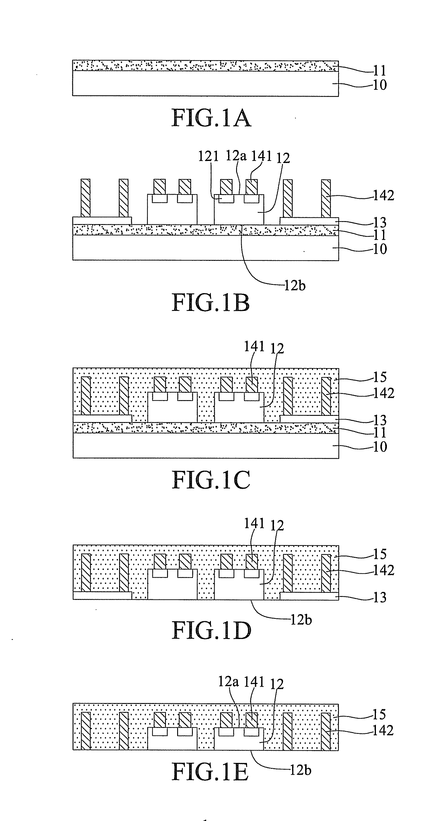
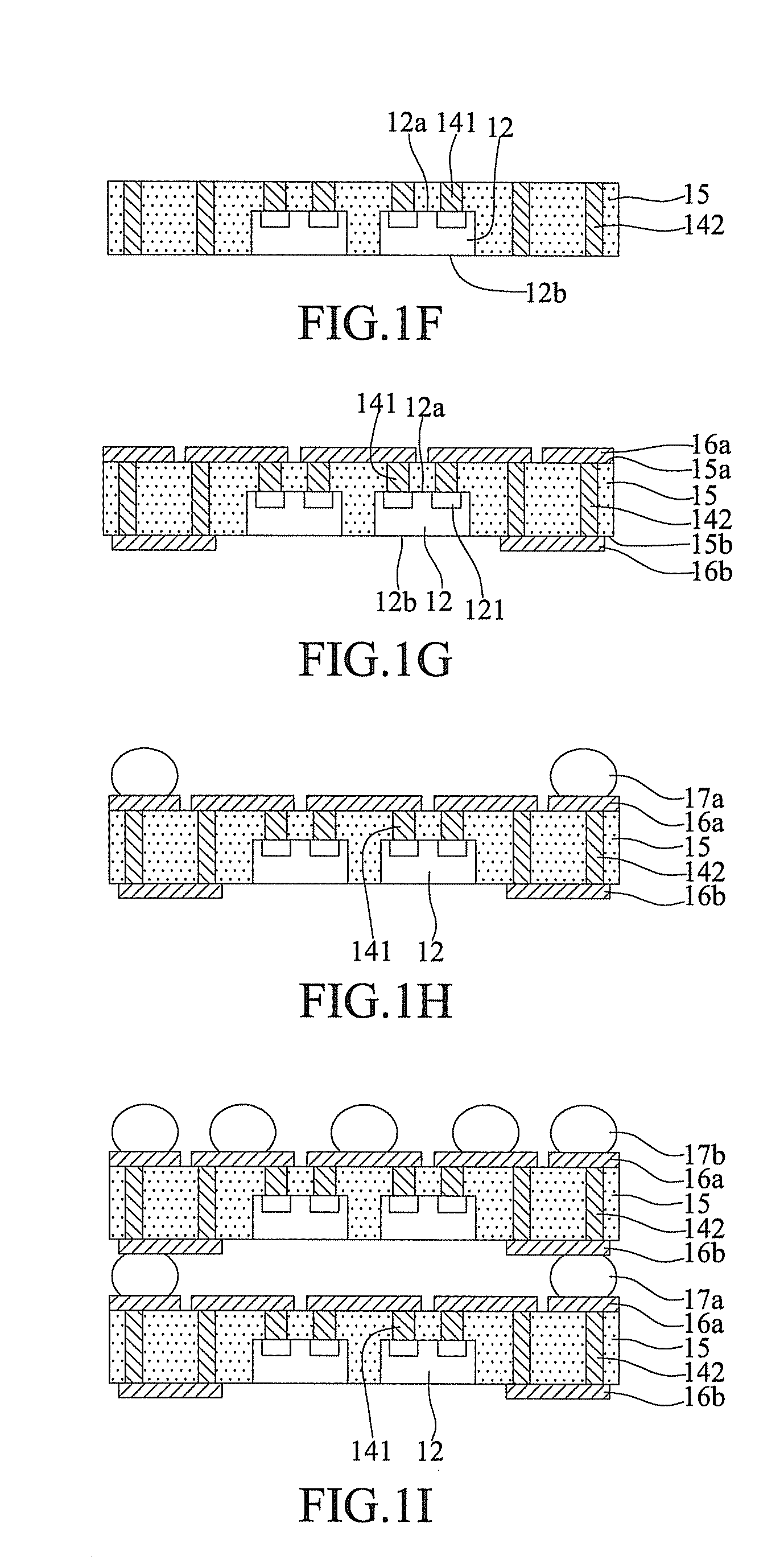
[0018]FIGS. 1A to 1I are schematic cross-sectional views showing a semiconductor package, a package structure and a fabrication method thereof according to the present invention.

[0019]Referring to FIG. 1A, an adhesive layer 11 is formed on a carrier 10. The adhesive layer 11 is a releasable adhesive tape, for example, an adhesive tape that loses its adhesive property when heated or exposed to UV light.

[0020]Referring to FIG. 1B, at least a semiconductor chip 12 such as a daisy chain chip and at least a sheet body 13 such as a dummy chip are mounted on the adhesive layer 11. The semiconductor chip 12 has an active surface 12a with a plurality of electrode pads 121 and a non-active surface 12b opposite to the active surface 12, and the semiconductor chip 12 is mounted on the adhesive layer 11 via the non-active surface 12b thereof. A plurality of first metal posts 141 are formed on the electrode pads 121 of the semiconductor chip 12 and a plurality of second metal posts 142 are formed...

second embodiment

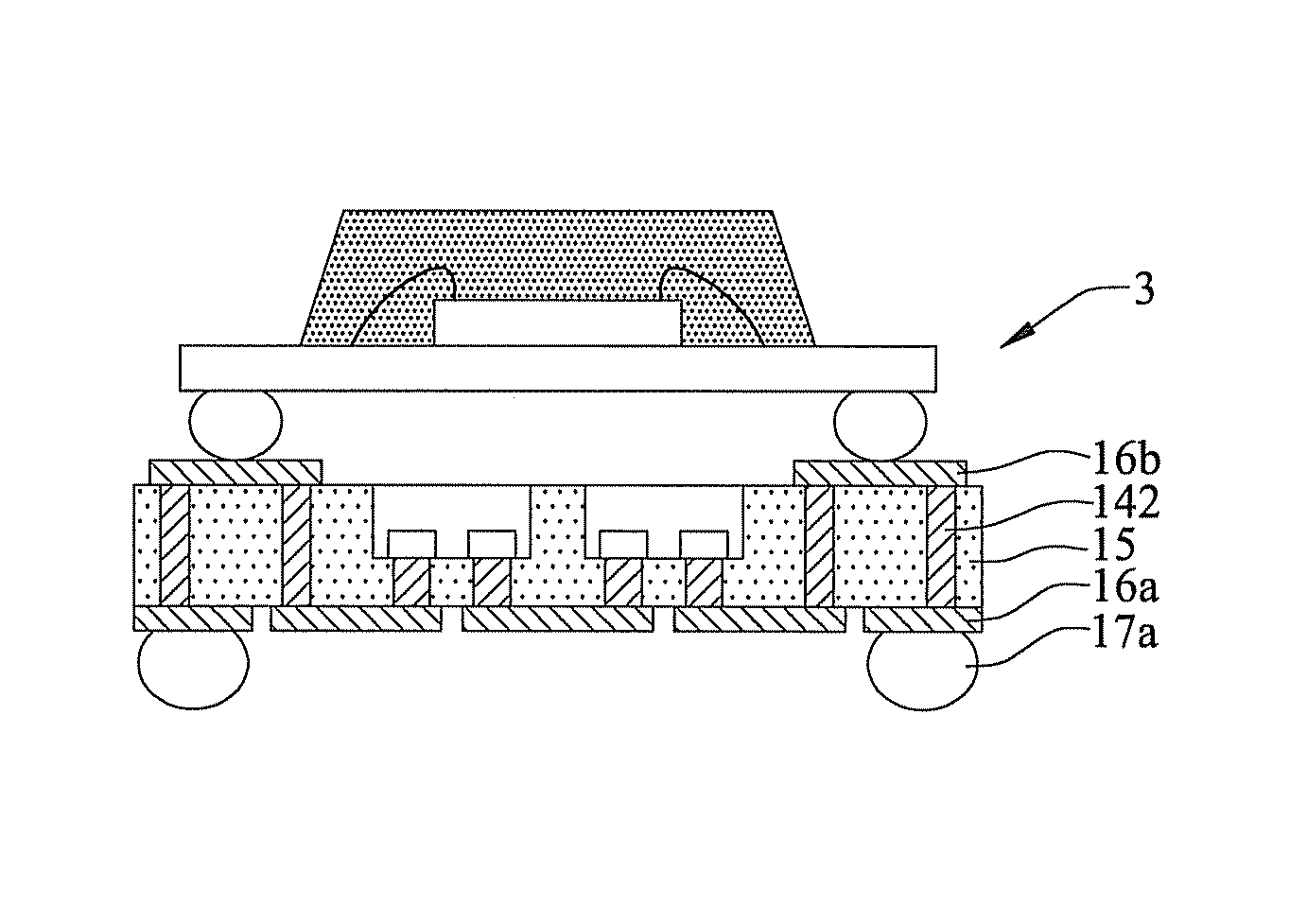
[0028]FIGS. 2A and 2B are schematic cross-sectional views showing a package structure according to the present invention. FIG. 2B shows another embodiment of FIG. 2A.

[0029]The second embodiment differs from the first embodiment in that a general semiconductor package is stacked on the first semiconductor package. Referring to FIG. 2A, a flip-chip semiconductor package 2 is stacked on the first semiconductor package and the second circuit layer 16b is used for electrically connecting a circuit board (not shown). Alternatively, referring to FIG. 2B, a wire bonding semiconductor package 3 is stacked on the first semiconductor package and the first circuit layer 16a is used for electrically connecting a circuit board (not shown). The present invention is not limited FIGS. 2A and 2B. For example, a chip-embedded semiconductor package (not shown) can be stacked on the first semiconductor package.

[0030]The present invention further provides a semiconductor package, which has: a dielectric ...


PUM


Abstract

A semiconductor package includes: a dielectric layer having opposite first and second surfaces; a semiconductor chip embedded in the dielectric layer and having a plurality of electrode pads; a plurality of first metal posts disposed on the electrode pads of the semiconductor chip, respectively, such that top ends of the first metal posts are exposed from the first surface; at least a second metal post penetrating the dielectric layer such that two opposite ends of the second metal post are exposed from the first and second surfaces, respectively; a first circuit layer formed on the first surface for electrically connecting the first and second metal posts; and a second circuit layer formed on the second surface for electrically connecting the second metal post. The semiconductor package dispenses with conventional laser ablation and electroplating processes for forming conductive posts in a molding compound, thereby saving fabrication time and cost.

Description

BACKGROUND OF THE INVENTION[0001]1. Field of the Invention[0002]The present invention relates to semiconductor packages, package structures and fabrication methods thereof, and, more particularly, to a semiconductor package, a package structure and a fabrication method thereof that dispense with a laser ablation process for forming through mold vias in a molding compound.[0003]2. Description of Related Art[0004]Currently, electronic products are developed towards miniaturization, multi-function, high performance and high operation speed. To meet the requirements of the electronic products, a plurality of semiconductor chips or packages are usually integrated in a semiconductor device.[0005]Generally, the number or size of the semiconductor chips in a semiconductor package should be increased so as to improve the overall performance and operation speed. On the other hand, the number and size of the semiconductor chips are limited by the size of substrates on which the semiconductor c...

Claims


Application Information

Patent Timeline
Patent Type & Authority Applications(United States)
IPC IPC(8): H01L23/498H01L21/50H01L21/56
CPCH01L24/24H01L2224/0401H01L2224/24137H01L2224/48227H01L2225/1035H01L2225/1058H01L2924/15311H01L2924/18162H01L23/3107H01L23/3128H01L21/561H01L21/568H01L25/105H01L24/11H01L24/14H01L24/81H01L2224/033H01L2224/1412H01L2224/81H01L23/5389H01L24/19H01L24/96H01L2224/04105H01L2224/12105H01L2924/15321H01L2924/15331H01L2224/16225H01L2924/181H01L2924/12042H01L2924/00H01L2924/00012
Inventor CHEN, YAN-HENGHUANG, JUNG-PANGLIAO, HSIN-YICHIU, SHIH-KUANGMA, GUANG-HWA
Owner SILICONWARE PRECISION IND CO LTD
Why Eureka
Try Eureka