Package structure with conformal shielding and inspection method using the same

a technology of shielding and packaging, applied in the direction of resistance/reactance/impedence, semiconductor/solid-state device details, instruments, etc., can solve the problems of increasing the amount of waste material and poor shielding performance, and achieve the effect of simple resistance meter and convenient inspection of emi (electromagnetic interference) shielding performan

Active Publication Date: 2013-10-03
UNIVERSAL SCI IND CO LTD +1
View PDF10 Cites 25 Cited by
  • Summary
  • Abstract
  • Description
  • Claims
  • Application Information

AI Technical Summary

Benefits of technology

[0005]The present invention has been accomplished under the circumstances in view. It is the main object of the present invention to provide a package structure with conformal shielding and inspection method using the same, which facilitates accurate examination of the EMI (electromagnetic interference) shielding performance of a package structure with a simple resistance meter without using an expensive X-ray scanner or destructing the product.

Problems solved by technology

However, a substrate cutting failure, uneven thickness of the conductive shielding layer or improper connection between the conductive shielding layer and the inner grounding structures may lead to poor shielding performance.
As a result, it needs to use an expensive X-ray scanner, or to destruct the finished product, increasing the amount of waste material.

Method used


Image

  • Package structure with conformal shielding and inspection method using the same
  • Package structure with conformal shielding and inspection method using the same
  • Package structure with conformal shielding and inspection method using the same

Examples


first embodiment

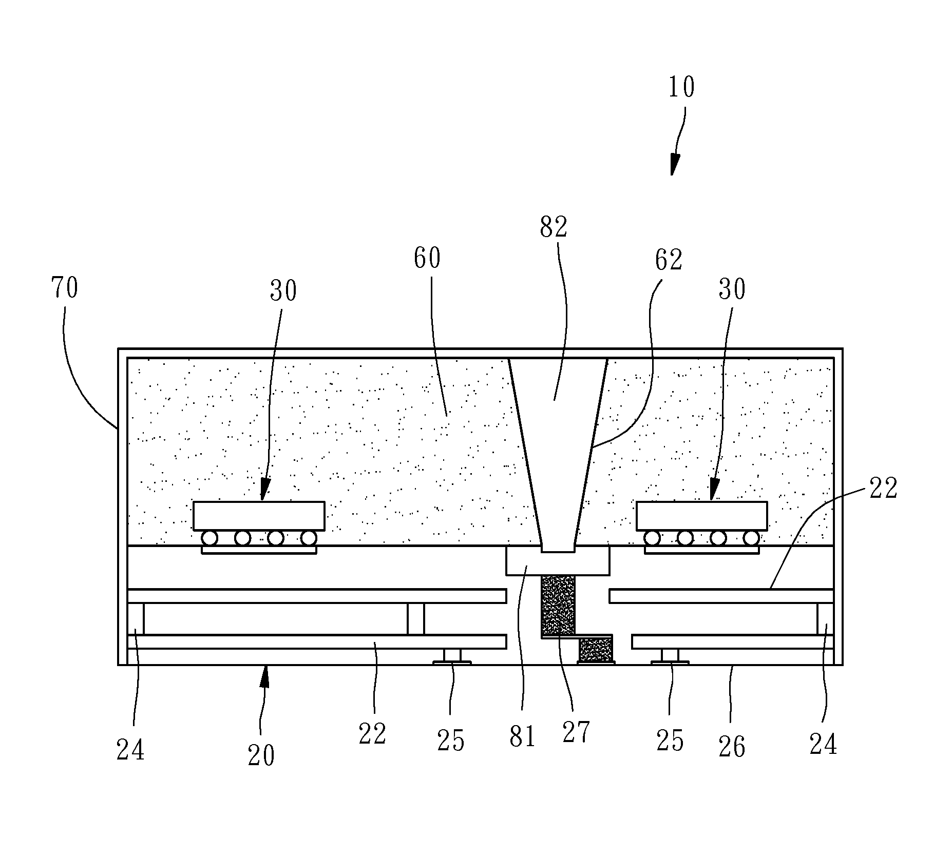
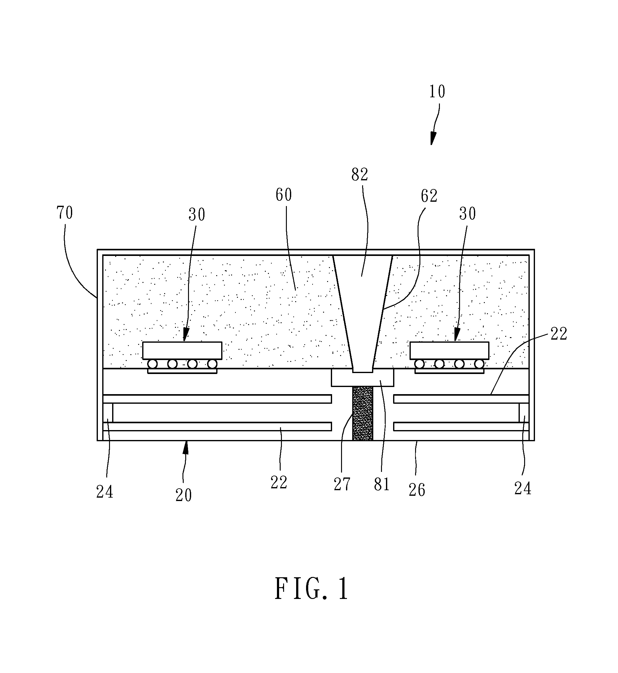
[0019]Referring to FIG. 1 through FIG. 4, a package structure with conformal shielding 10 in accordance with the present invention is shown. The package structure with conformal shielding 10 comprises a substrate 20, at least one, for example, two chip modules 30 mounted on the substrate 20, a molding compound 60 covering the chip modules 30, and a conductive shielding layer 70 covering the molding compound 60 and the lateral sides of the substrate 20.

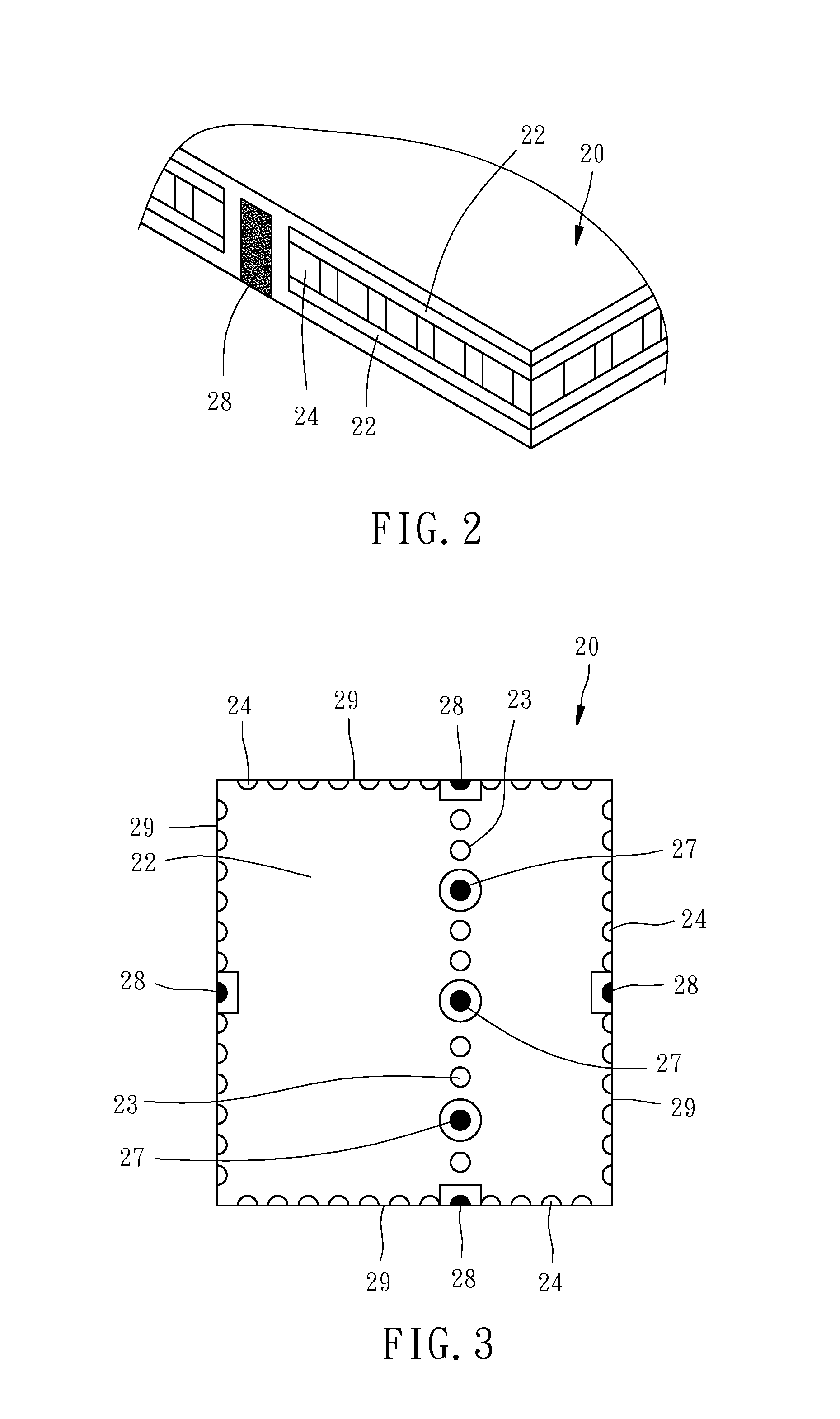
[0020]The substrate 20 is similar to a conventional multilayer PC board, comprising at least one ground layer 22 set therein, and a plurality of inner grounding structures 23, 24 inserted through respective ground vias therein and electrically connected to the at least one ground layer 22. The aforesaid ground vias can be through holes, blind holes, countersunk holes, or other similar structures and their combinations. Further, the inner grounding structures 23, 24 can be any of a variety of conductive connection components and their c...

second embodiment

[0033]Further, in this second embodiment, the independent conducting structures 27, 28 can be formed of multiple segments without departing from the spirit and scope of the invention.

[0034]By means of the package structure with conformal shielding 10 and inspection method provided by the present invention, the EMI (electromagnetic interference) shielding performance of the package structure 10 can be examined quickly with a simple resistance meter without using an expensive X-ray scanner or destructing the product. Thus, all the products can be inspected individually, avoiding possible errors in sampling inspection.


PUM


Abstract

A package structure with conformal shielding includes a substrate providing electrically connected inner grounding structures, a chip module mounted on the substrate, a molding compound covering the chip module and one surface of the substrate, and a conductive shielding layer covering the molding compound and the lateral sides of the substrate, and electrically connected with a part of the inner grounding structures. The substrate further provides one or multiple independent conductive structures electrically connected with the conductive shielding layer and exposed to the outside. By measuring the resistance value between one independent conductive structure and the conductive shielding layer or another independent conductive structure or one ground contact and then comparing the measured resistance value with a predetermined reference value, the EMI shielding performance of the package structure is determined.

Description

BACKGROUND OF THE INVENTION[0001]1. Field of the Invention The present invention relates to EMI (electromagnetic interference) shielding technology of using conformal shielding in package process to prevent EMI and more particularly, to a package structure with conformal shielding and inspection method using the same that is practical for conformal shielding application as well as compartment shielding application.[0002]2. Description of the Related Art[0003]The technique of conformal shielding is to form a conductive shielding layer on the periphery of an electronic module by means of sputtering, spray coating or any other film coating technique. Prior to the film coating step, the fabrication of the electronic module employs a substrate cutting step. After the substrate cutting step, many inner grounding structures are exposed to the outside of the substrate. After covered on the module, the conductive shielding layer is electrically connected with the inner grounding structures t...

Claims


Application Information

Patent Timeline
Patent Type & Authority Applications(United States)
IPC IPC(8): G01R27/08H01L23/552
CPCG01R1/0433H01L23/552G01R31/2896H01L2224/16225G01R31/002
Inventor DING, JAW-MINGLIU, CHIEN-YEHCHIANG, CHIH-HAO
Owner UNIVERSAL SCI IND CO LTD
Why Eureka
Try Eureka