Display Device and Electronic Device

Inactive Publication Date: 2013-10-10
SEMICON ENERGY LAB CO LTD
View PDF15 Cites 38 Cited by
  • Summary
  • Abstract
  • Description
  • Claims
  • Application Information

AI Technical Summary

Benefits of technology

[0035]According to the present invention, a display device that can display an image which causes a

Problems solved by technology

Thus, there has been a problem in that the

Method used


Image

  • Display Device and Electronic Device
  • Display Device and Electronic Device
  • Display Device and Electronic Device

Examples


embodiment 1

[0050]In this embodiment, a configuration example of a display device of one embodiment of the present invention is described with reference to drawings.

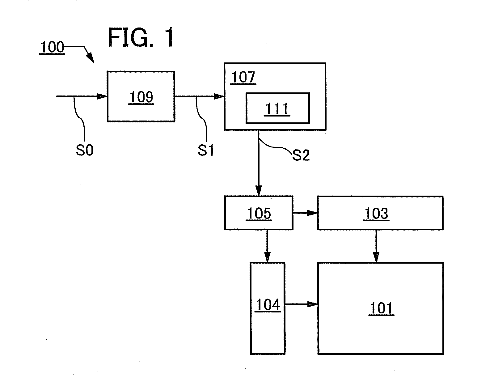
[0051]FIG. 1 is a block diagram illustrating a configuration example of a display device according to one embodiment of the present invention.

[0052]A display device 100 includes a display portion 101, a driver circuit portion 103, a driver circuit portion 104, a control circuit portion 105, an image processing device 107, and a decoder circuit portion 109.

[0053]The decoder circuit portion 109 is inputted with an image signal S0 which is compressed or encoded, decodes the image signal S0, and converts it into a first image signal S1. The first image signal S1 converted here is transmitted to the image processing device 107.

[0054]The image processing device 107 converts the inputted first image signal S1 into a second image signal S2 containing image data which is proper to display in the display portion 101.

[0055]The image processing...

embodiment 2

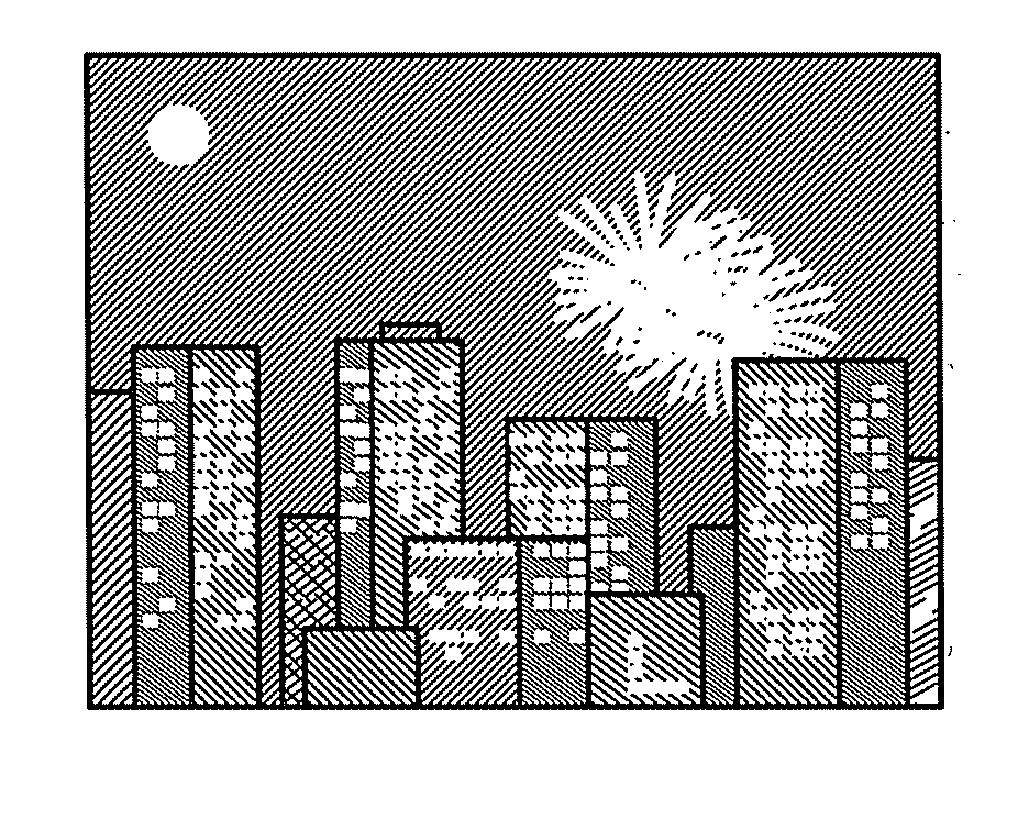
[0164]In this embodiment, a method in which an image contained in an inputted image signal is divided into a plurality of regions and grayscale conversion processing is performed only to the region which needs the processing is described.

[0165]An image contained in the first image signal S1 inputted to the grayscale conversion portion 111 is divided into a plurality of regions, and each luminance distribution in the regions is extracted. In addition, the grayscale conversion portion 111 determines whether to perform grayscale conversion processing to the regions based on the extracted luminance distribution.

[0166]The grayscale conversion portion 111 performs the above-described grayscale conversion processing to a region which is determined to be subjected to grayscale conversion processing, whereas grayscale in a region where grayscale conversion processing is not performed remains unchanged.

[0167]Then, the grayscale conversion portion 111 integrates the regions where grayscale con...

embodiment 3

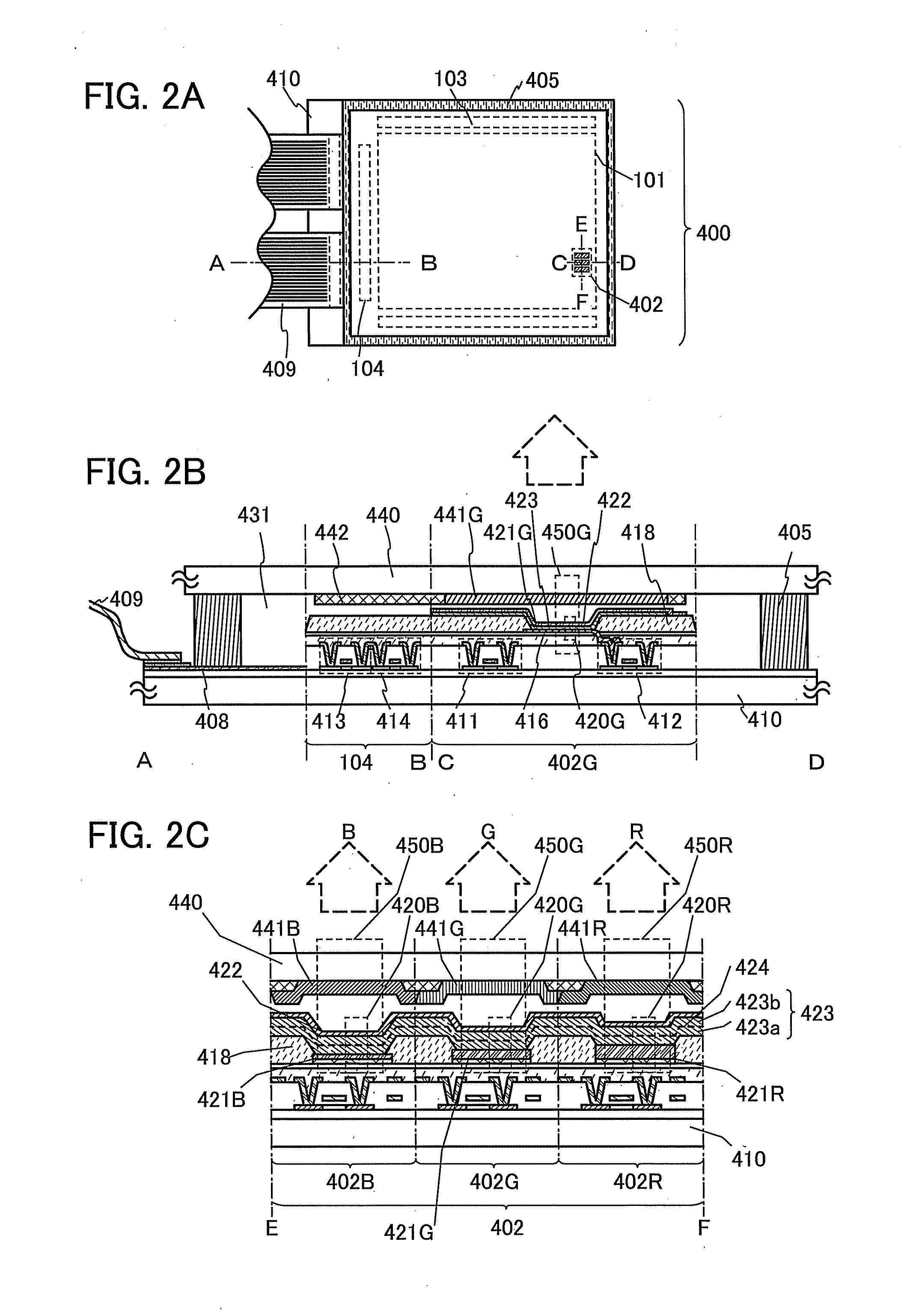
[0185]In this embodiment, the structure of a light-emitting element which can be used for the light-emitting module according to an embodiment of the present invention is described with reference to FIGS. 7A to 7C.

[0186]The light-emitting element described in this embodiment as an example includes a first electrode, a second electrode, and a layer containing a light-emitting organic compound (hereinafter referred to as an EL layer) provided between the first electrode and the second electrode. One of the first electrode and the second electrode functions as an anode, and the other functions as a cathode. The EL layer is provided between the first electrode and the second electrode, and a structure of the EL layer may be appropriately selected in accordance with materials of the first electrode and second electrode.

[0187]An example of the structure of the light-emitting element is illustrated in FIG. 7A. The light-emitting element exemplified in FIG. 7A includes an EL layer formed of...


PUM


Abstract

A dark portion in an image seen by a viewer is expressed more precisely, whereby the image given a greater sense of depth is displayed. A display device in which pixels each include a light-emitting module capable of emitting light having a spectral line half-width of less than or equal to 60 nm in a response time of less than or equal to 100 μs and are provided at a resolution of higher than or equal to 80 ppi; the NTSC ratio is higher than or equal to 80%; and the contrast ratio is higher than or equal to 500, is provided with a circuit converting an image signal having a given grayscale into an image signal capable of representing an image on the low luminance side by high-level grayscale.

Description

TECHNICAL FIELD[0001]The present invention relates to a display device. The present invention relates to an electronic device including a display device.BACKGROUND ART[0002]A display device that displays a stereoscopic image using a binocular parallax is known. Such a display device is configured to display, on one screen, an image to be seen from the position of the left eye of a viewer (an image for left eye) and an image to be seen from the position of the right eye of the viewer (an image for right eye). The viewer sees the image for left eye with the left eye and the image for right eye with the right eye and is thus allowed to see a stereoscopic image.[0003]For example, in a glasses system, an image for left eye and an image for right eye are alternately displayed on a screen of a display device in synchronization with a shutter provided in a pair of glasses, whereby the left eye of a viewer is allowed to see only the image for left eye and the right eye of the viewer is allow...

Claims


Application Information

Patent Timeline
IPC IPC(8): G09G5/02H04N13/122
CPCG09G5/02H04N13/0018H04N13/0033G06F3/0421H01L27/322G09G3/3208G09G2320/0271H01L51/5265H01L51/5278G09G3/003G09G3/20G09G2360/16C09K11/06C09K2211/185H04N13/122H04N13/144H10K59/38H10K50/852H10K50/19G09F9/30G09G3/30H05B33/12H05B33/24H10K50/00H10K59/00
Inventor YAMAZAKI, SHUNPEIHIRAKATA, YOSHIHARU
Owner SEMICON ENERGY LAB CO LTD
Why Eureka
Try Eureka