
Liquid crystal display device

a liquid crystal display and display device technology, applied in non-linear optics, instruments, optics, etc., can solve the problems of significantly deteriorating transmittance and deteriorating image quality, and achieve high transmittance, prevent generation, and high definition

Active Publication Date: 2013-10-10
JAPAN DISPLAY INC
View PDF4 Cites 4 Cited by
  • Summary
  • Abstract
  • Description
  • Claims
  • Application Information

AI Technical Summary

Benefits of technology

The present invention provides a liquid crystal display device with a wall electrode (IPS type) that prevents the generation of domains within the pixel and maintains high transmittance and brightness, even at higher definition screens. This improves the efficiency of the display mode and reduces the voltage applied to the pixel, resulting in high definition screen with high transmittance.

Problems solved by technology

This may cause contamination between those pixels, resulting in deteriorated image quality.
As a result, the transmittance distribution in the pixel becomes inhomogeneous, thus causing the problem of significantly deteriorating the transmittance.

Method used


Image

  • Liquid crystal display device
  • Liquid crystal display device
  • Liquid crystal display device

Examples


first embodiment

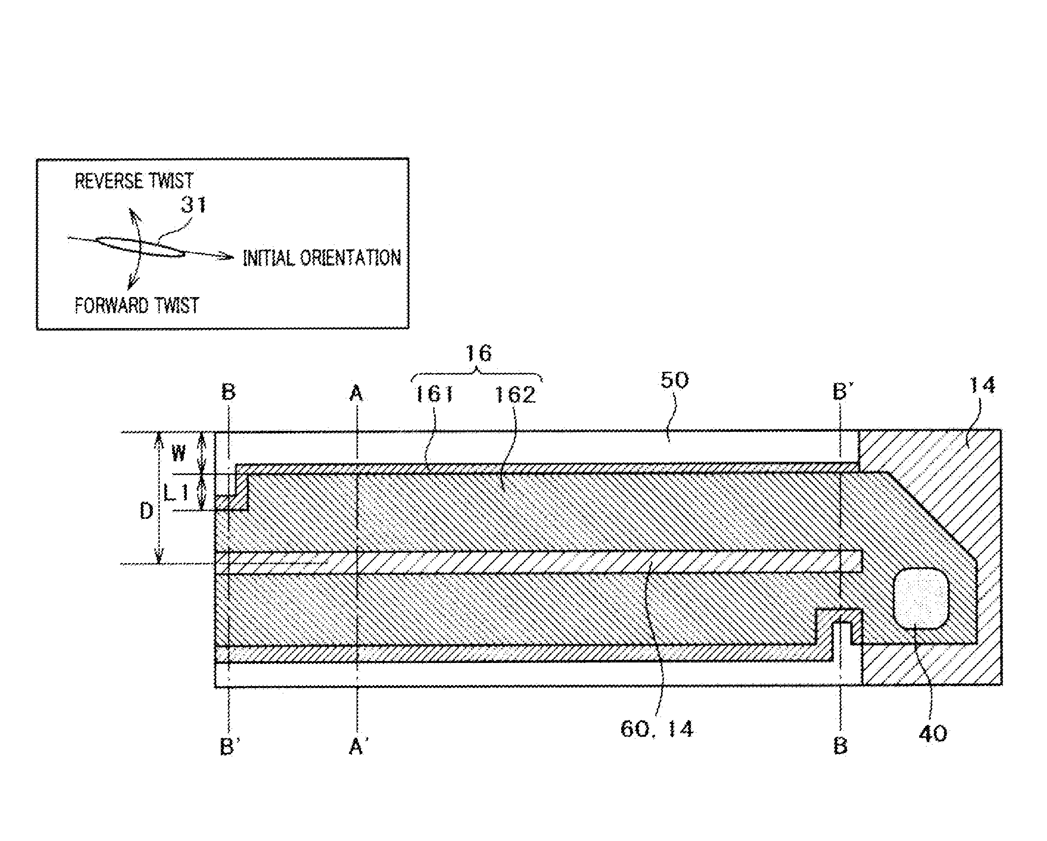
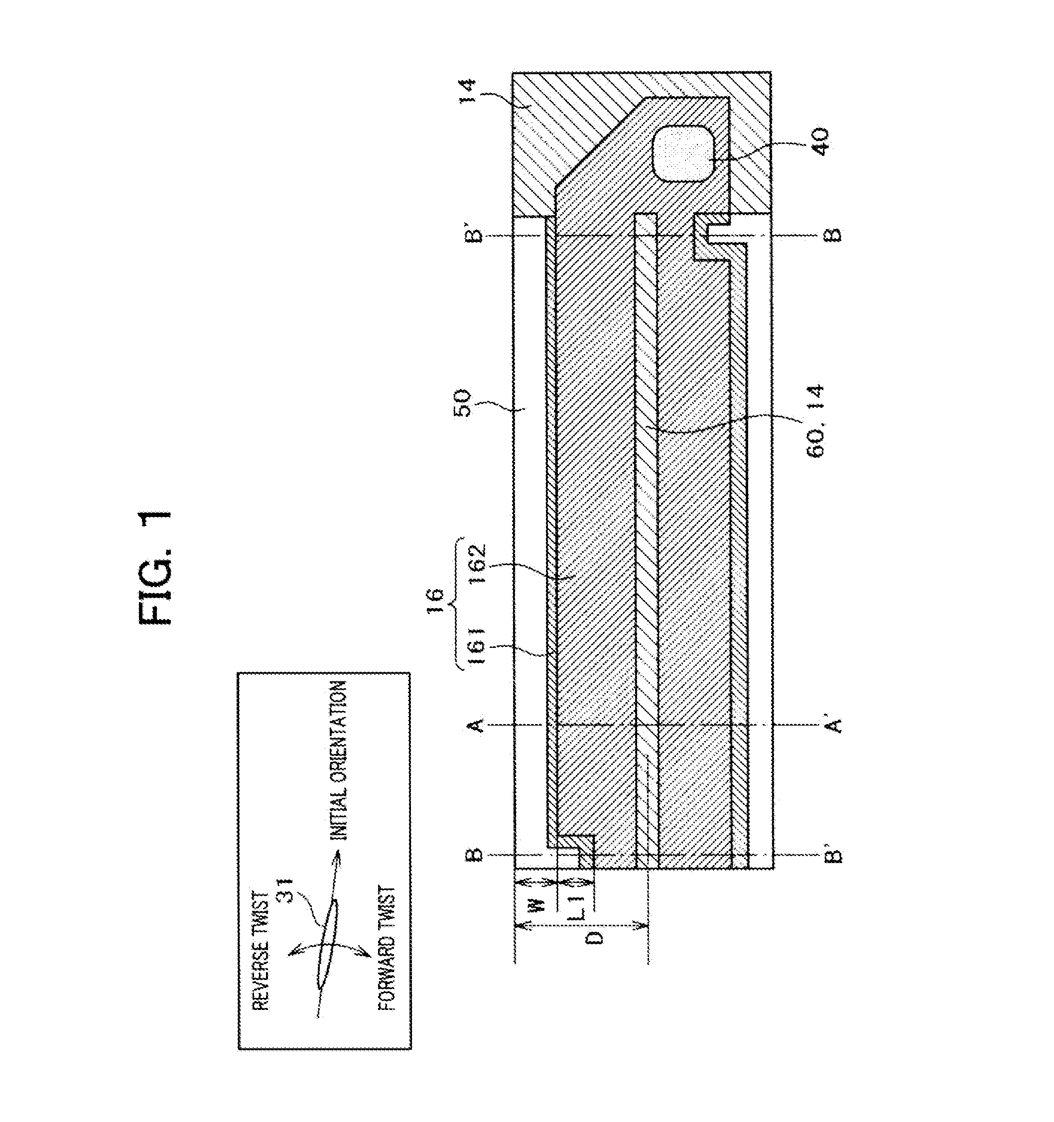
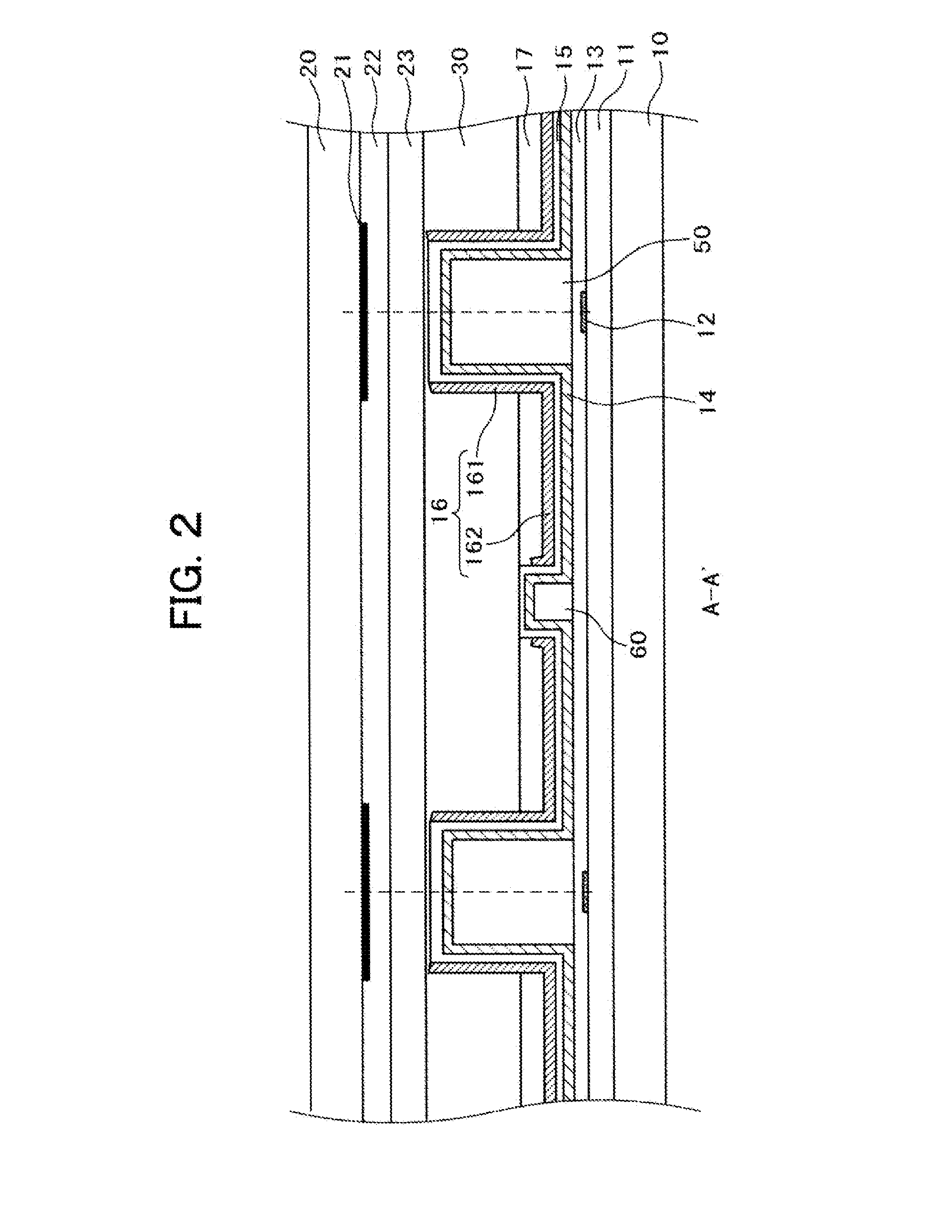
[0034]FIG. 1 shows a structure of a pixel according to the present invention as a plan view. FIG. 2 is a cross-section taken on line A-A′ of FIG. 1. FIG. 3 is a cross section taken on line B-B′ of FIG. 1. As FIG. 1 shows, the pixel according to the present invention has different cross section structures between the area around the center of the pixel (taken on line A-A′) and the area around the end part of the pixel (taken on line B-B′).

[0035]Referring to FIG. 1, a small wall 60 transversely extends along the center of the pixel. Large walls 50 transversely extend at the boundary of the pixel while interposing the small wall 60. A common electrode 14 is formed on the upper surface of the small wall 60. A wall electrode 161 is formed at the inner side of the large wall 50, and a plane electrode 162 is formed between the small wall 60 and the large wall 50. A pixel electrode 16 is formed of the wall electrode 161 and the plane electrode 162. A through hole 40 for connecting a video s...

second embodiment

[0053]FIG. 7 is a plan view of the pixel according to a second embodiment of the present invention. FIG. 8 is a cross section taken on line C-C′ of FIG. 7. The cross section taken on line A-A′ of FIG. 7 is the same as the one used for explanation referring to FIG. 2. Referring to FIG. 7, like the first embodiment, the width of the large wall 50 is increased at the end part of the pixel, and the wall electrode 161 is bent toward the center of the pixel. The characteristic of the embodiment is that the small wall 60 is bent in the direction where the wall electrode 161 is bent in association with increase in the width of the large wall 50 as shown in FIG. 7. In other words, the small wall 60 is bent at the area around where the pixel electrode 161 is bent in the direction away from the bent pixel electrode 161.

[0054]FIG. 8 is a cross section taken on line C-C′ of FIG. 7 representing a structure of the end part of the pixel. As FIG. 8 shows, one of the large walls 50 has the larger wid...

third embodiment

[0060]FIG. 12 is a plan view of a pixel according to a third embodiment of the present invention. The structure shown in FIG. 12 is configured by extending the bent structure of the common electrode 14 formed on the small, wall 60 as shown in FIG. 7 according to the second embodiment to the area around the through hole 40 at the end part of the pixel. Extending the common electrode 14 formed on the small wall 60 to the area around the through hole 40 allows the liquid crystal around the through hole 40 to serve as the display region, thus improving the transmittance.

[0061]As FIG. 12 shows, the structure has the bent small wall 60, which allows the liquid crystal molecule 31 to be twisted forward in the liquid crystal layer around the through hole 40, suppressing generation of the domain. That is, the transmission region may be widened while suppressing generation of the domain, resulting in improved transmittance. A region A enclosed by the dashed line as shown in FIG. 12 serves as ...


PUM

PropertyMeasurementUnit
heightaaaaaaaaaa
thicknessaaaaaaaaaa
areaaaaaaaaaaa

Abstract

The liquid crystal display device includes a pixel structure provided with a large wall formed along a long side of a pixel with a rectangular plane, a small wall formed at a center of the pixel and extending in the same direction as the large wall, a wall electrode formed on a wall surface of the large wall, a plane electrode formed between the small and large walls, in which the wall electrode and the plane electrode form a pixel electrode, and a common electrode formed on a surface of the small wall. The large wall has a part with an increased thickness at an end part of the pixel. The wall electrode is bent toward the center of the pixel. This structure prevents decrease of reverse twist of liquid crystal at an end part of the pixel as well as generation of domain, thus improving the transmittance of the screen.

Description

CLAIM OF PRIORITY[0001]The present application claims priority from Japanese Patent Application JP 2012-086872 filed on Apr. 10, 2012, the content of which is hereby incorporated by reference into this application.BACKGROUND OF THE INVENTION[0002]1. Technical Field[0003]The present invention relates to a display device, and more particularly, the present invention relates to an IPS type liquid crystal display device with excellent viewing angle property, which is capable of realizing a high-definition screen.[0004]2. Related Art[0005]The liquid crystal display panel, used for the liquid crystal display device includes a TFT substrate having pixels with pixel electrodes and thin film transistors (TFT) arranged in a matrix, a counter substrate that faces the TFT substrate and has color filters at positions corresponding to the pixel electrodes of the TFT substrate, and a liquid crystal interposed between the TFT substrate and the counter substrate. The image is generated by controllin...

Claims


Application Information

Patent Timeline
Patent Type & Authority Applications(United States)
IPC IPC(8): G02F1/1343
CPCG02F1/133707G02F1/134363G02F1/133377G02F1/1343
Inventor HIRATSUKA, TAKATOITOU, OSAMUYAMAMOTO, MASANAOSONODA, DAISUKE
Owner JAPAN DISPLAY INC
Learn More