Housing and Method for Producing a Housing

a housing and housing technology, applied in the field of housing, can solve the problems of too complicated and cost-intensive for consumer markets, and achieve the effects of simple and cost-effective production, simple and reliable production, and good heat dissipation of radiation-generating semiconductor chips

Active Publication Date: 2013-10-10
OSRAM OLED
View PDF5 Cites 2 Cited by
  • Summary
  • Abstract
  • Description
  • Claims
  • Application Information

AI Technical Summary

Benefits of technology

[0004]Embodiments of the invention specify a housing for an optoelectronic semiconductor component which can be produced simply and cost-effectively and at the same time ensures good heat dissipation from the radiation-generating semiconductor chip. Further embodiments specify a method by which a housing can be produced simply and reliably.

Problems solved by technology

On account of the comparatively complicated construction of these metal housings, however, the latter are too complicated and cost-intensive for uses in the consumer market.

Method used


Image

  • Housing and Method for Producing a Housing
  • Housing and Method for Producing a Housing
  • Housing and Method for Producing a Housing

Examples


Embodiment Construction

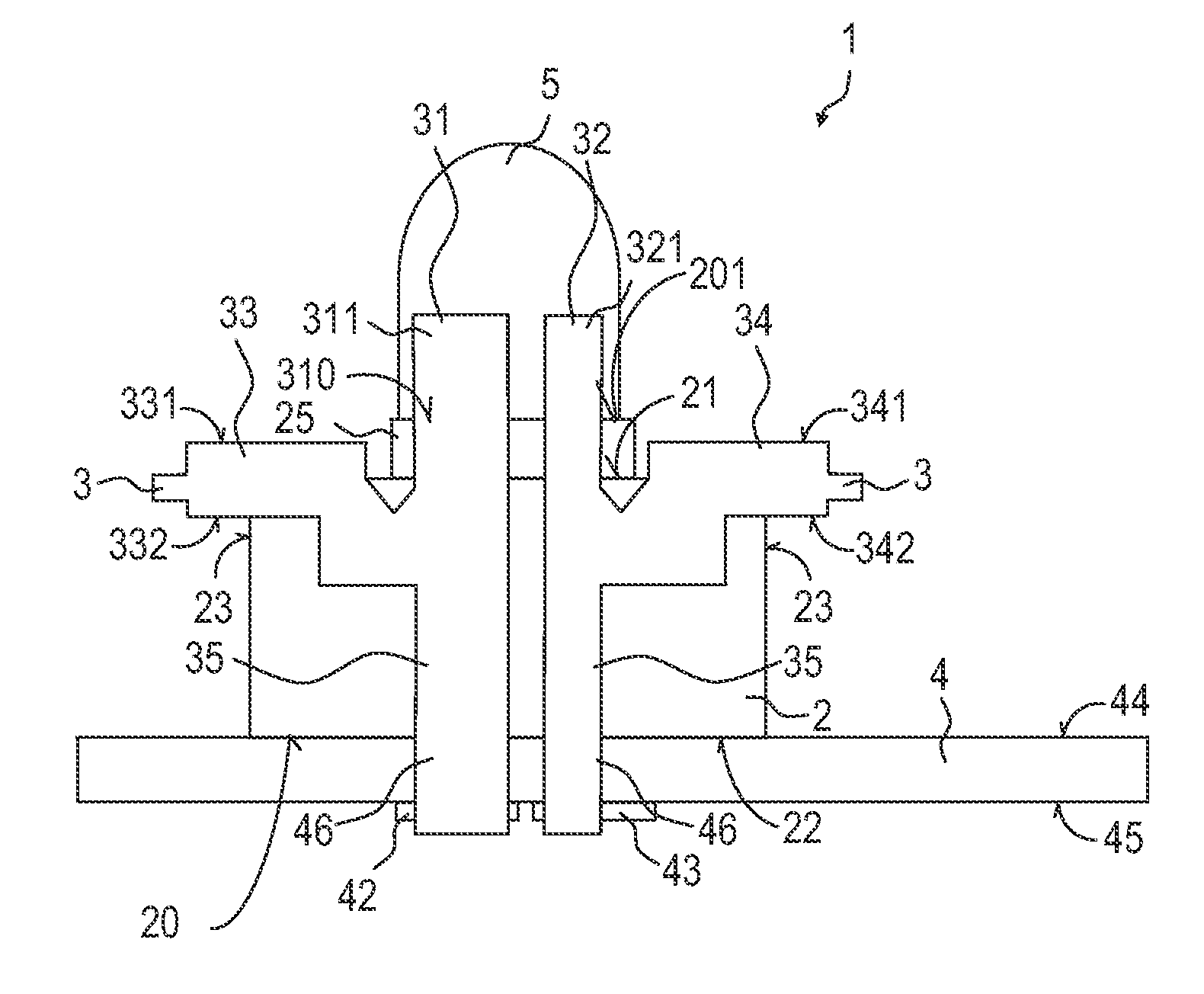
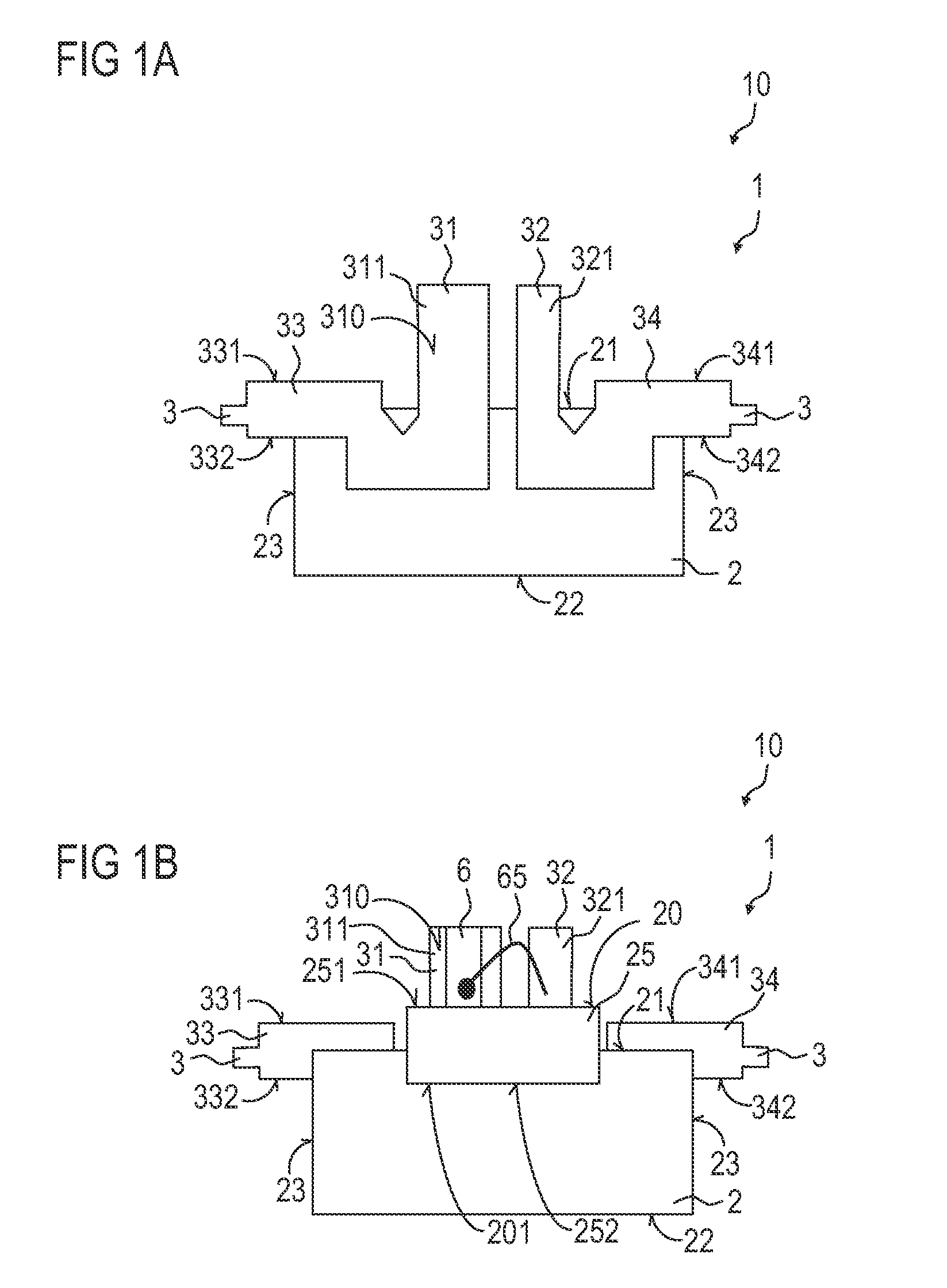
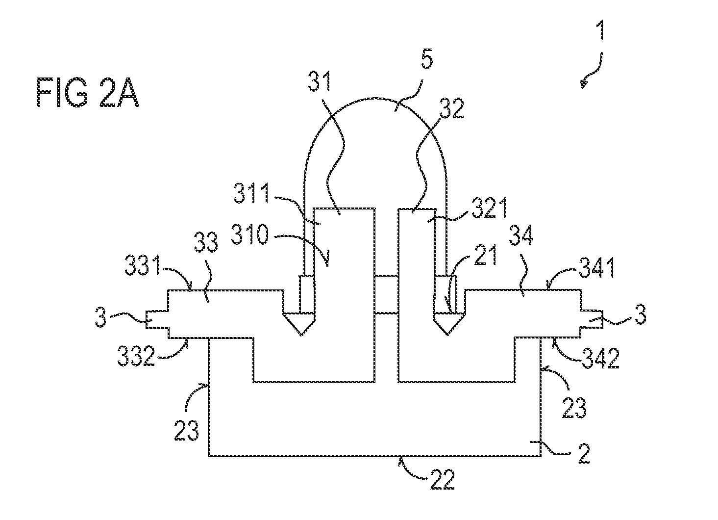
[0050]FIGS. 1A and 1B schematically illustrate a first exemplary embodiment of a housing 1 for a surface-mountable semiconductor component 10.

[0051]The housing 1 comprises a first connection conductor 31 and a second connection conductor 32. The connection conductors form a leadframe 3, onto which a housing body 2 is molded. The housing body is produced from a plastic. The housing body 2 extends in a vertical direction in regions between a first main face 21 and a second main face 22. A region 311 of the first connection conductor 31 and a region 321 of the second connection conductor 32 in each case project from the first main face 21 of the housing body 2. The projecting regions of the connection conductors run parallel to one another. The projecting regions are provided for making electrical contact with a semiconductor chip.

[0052]The leadframe 3 extends in planar fashion along a main extension plane. The connection conductors 31, 32 therefore run in a common plane. The main exte...


PUM


Abstract

A housing for an optoelectronic semiconductor component includes a housing body having a mounting plane and a leadframe with a first connection conductor and a second connection conductor. The housing body deforms the leadframe in some regions. The leadframe has a main extension plane which extends obliquely or perpendicularly with respect to the mounting plane. A semiconductor component having such a housing and a semiconductor chip and a method for producing a housing are also disclosed.

Description

[0001]This patent application is a national phase filing under section 371 of PCT / EP2011 / 065842, filed Sep. 13, 2011, which claims the priority of German patent application 10 2010 046 088.5, filed Sep. 20, 2010, each of which is incorporated herein by reference in its entirety.TECHNICAL FIELD[0002]The present application relates to a housing, a semiconductor component comprising such a housing, and a method for producing a housing.BACKGROUND[0003]For semiconductor laser diodes having waste heat powers into the watts range, so-called TO housings, for example TO56, TO38 or TO9 housings, are often used. On account of the comparatively complicated construction of these metal housings, however, the latter are too complicated and cost-intensive for uses in the consumer market.SUMMARY OF THE INVENTION[0004]Embodiments of the invention specify a housing for an optoelectronic semiconductor component which can be produced simply and cost-effectively and at the same time ensures good heat dis...

Claims


Application Information

Patent Timeline
Patent Type & Authority Applications(United States)
IPC IPC(8): H01S5/024H01L23/495H01S5/0232H01S5/02375
CPCH01L33/62H01S5/02216H01L2224/48465H01L2224/48091H01S5/024H01L23/495H01S5/02244H01S5/02276H01S5/02288H01S5/02296H01S5/02476H01L2924/00014H01L2924/00H01S5/0231H01S5/02345H01S5/02257H01S5/02253H01S5/02375H01S5/0232H01S5/02208H05K5/0091
Inventor STRAUSS, UWEARZBERGER, MARKUS
Owner OSRAM OLED
Why Eureka
Try Eureka