Opto-electronic device assembly
- Summary
- Abstract
- Description
- Claims
- Application Information
AI Technical Summary
Benefits of technology
Problems solved by technology
Method used
Image
Examples
Embodiment Construction
[0039]Reference will now be made in detail to the preferred embodiment of the present invention.
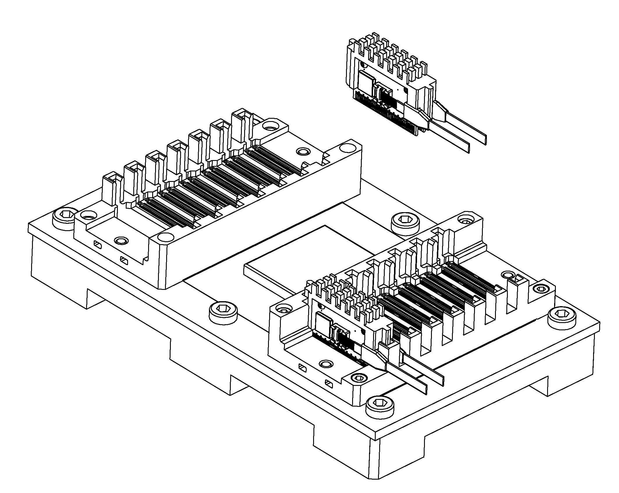
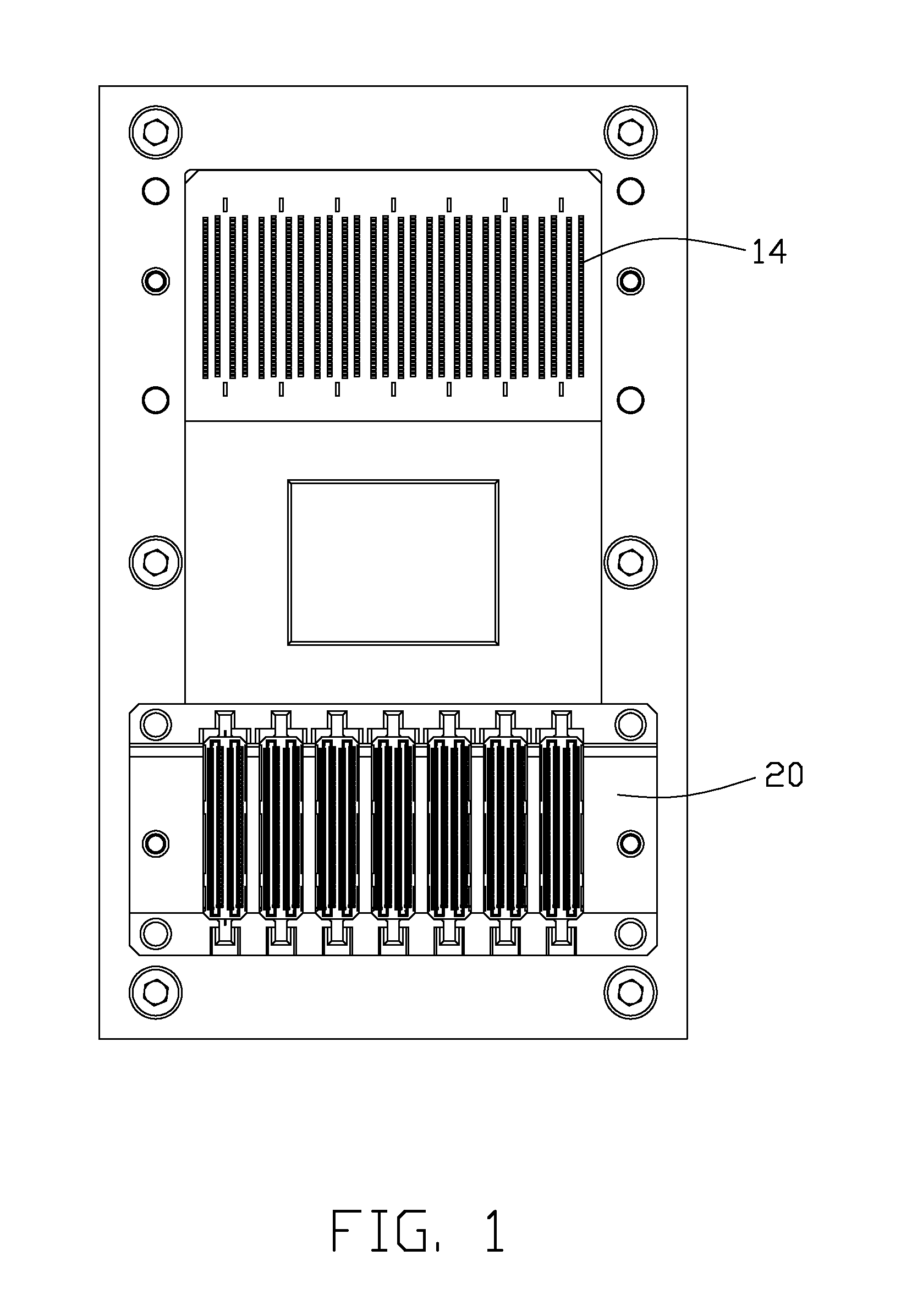
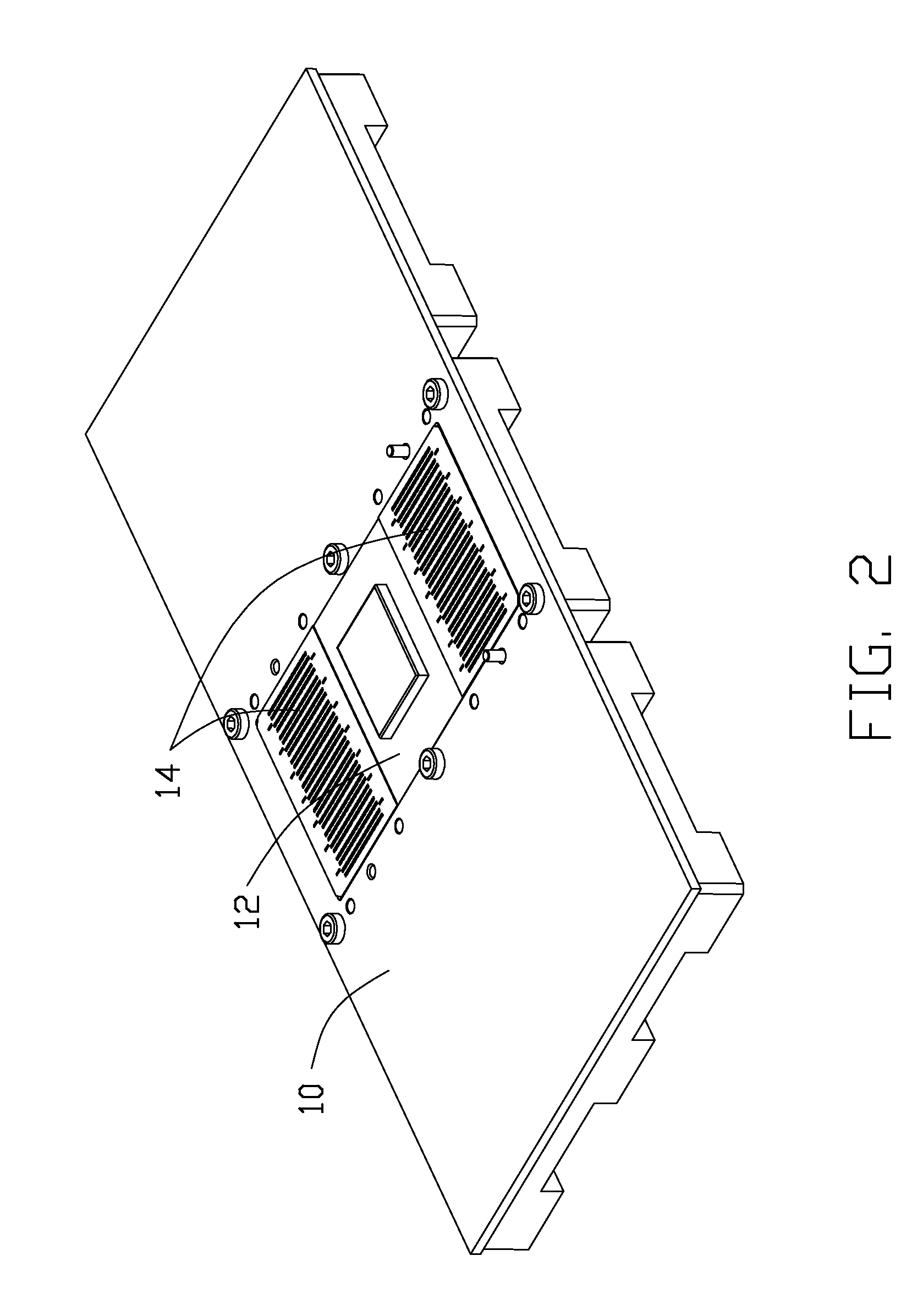
[0040]Referring FIGS. 1-24, an aluminum frame 10 defines a ceramic substrate receiving area to receive a ceramic substrate 12 therein. The ceramic substrate 12 defines two connector areas 14, on two opposite ends in a longitudinal direction, forming LGA (Land Grid Array) pads 16 thereon. A modular SLC (Surface Laminar Circuit) interconnect system 18 is fastened to the aluminum frame 10 around each of the connector areas 14, and includes an aluminum organizer 20 defining a plurality of elongated cavities 22 in a transverse direction perpendicular to the longitudinal direction while each of the cavities 22 extends along the longitudinal direction. The aluminum organizer 20 defines a plurality of fastening holes 24 and a plurality of locating holes 26 to receive corresponding screws 28 and dowel pins 30 for locating and fastening the organizer 20 upon the aluminum frame 10. The organizer 20 ...
PUM
 Abstract
Description
Claims
Application Information


