Bipolar transistor manufacturing method

a manufacturing method and technology of bipolar transistor, applied in the direction of transistors, electrical devices, semiconductor devices, etc., can solve the problems of mos transistor manufacturing methods, 1 is its bulk, and the depth is not compatible with the latest methods for manufacturing mos transistors, and achieves high frequency performan

Inactive Publication Date: 2013-10-17
STMICROELECTRONICS SRL
View PDF5 Cites 21 Cited by
  • Summary
  • Abstract
  • Description
  • Claims
  • Application Information

AI Technical Summary

Benefits of technology

[0024]One or more embodiments provide a method for manufacturing an integrated bipolar transistor having a very high frequency performance.

Problems solved by technology

A first disadvantage of a bipolar transistor such as that in FIG. 1 is its bulk.
Such a depth is not compatible with recent methods for manufacturing MOS transistors on substrates of silicon-on-insulator type (SOI) where the upper substrate is very thin (thickness smaller than 15 nm).
It should be noted that the forming of single-crystal silicon for the access to the base is not compatible with the above method, a growth or a deposition of single-crystal silicon being impossible to perform on an insulating material.
Thus, the bipolar transistor of FIG. 1 has junction capacitances and access resistances which are generally not compatible with a high-performance bipolar transistor.

Method used


Image

  • Bipolar transistor manufacturing method
  • Bipolar transistor manufacturing method
  • Bipolar transistor manufacturing method

Examples


Embodiment Construction

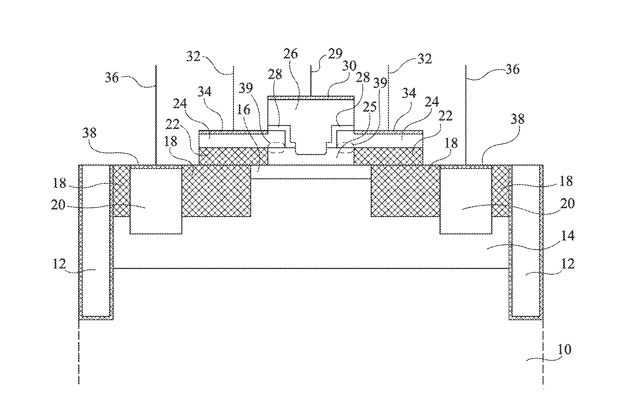
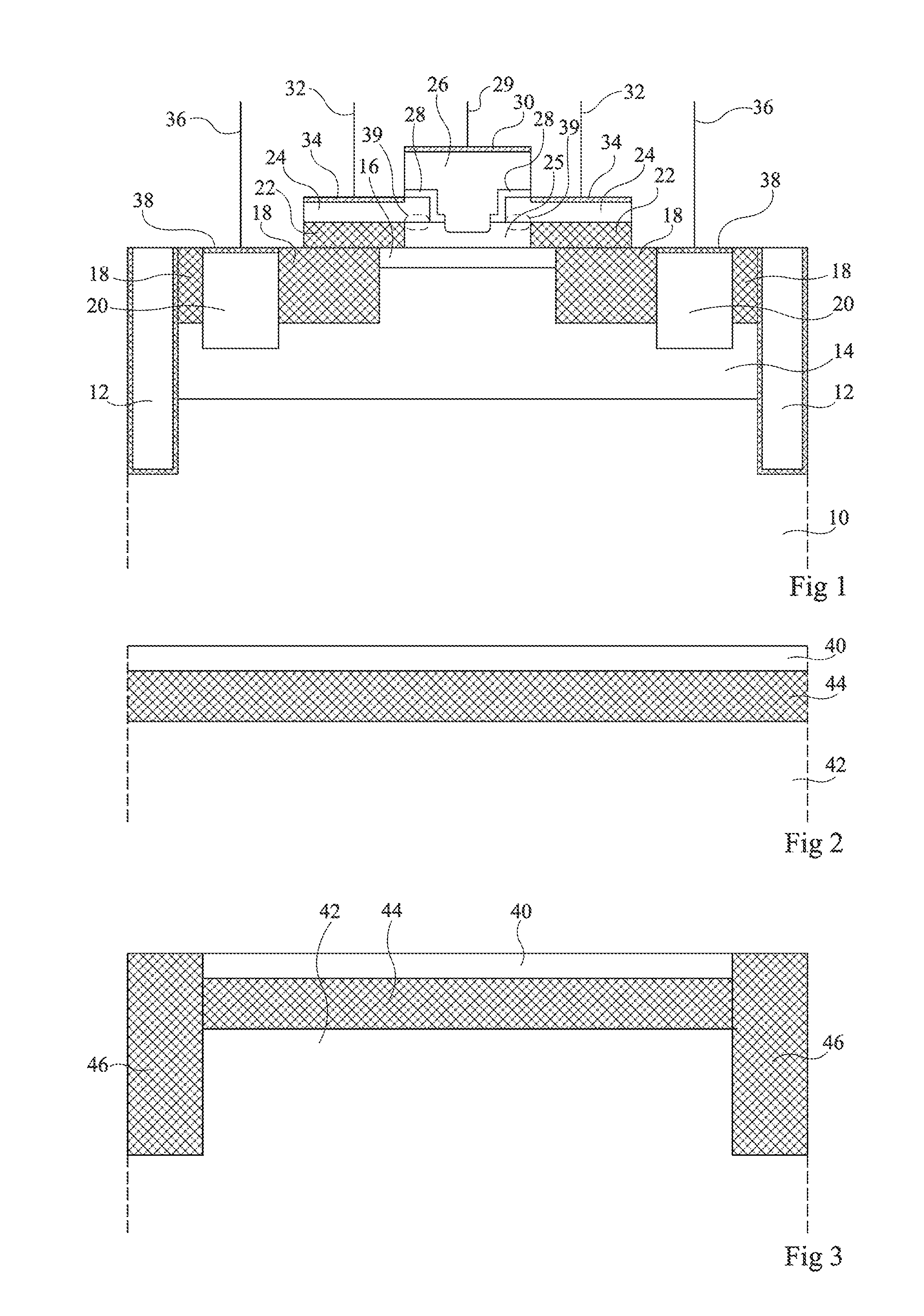
[0044]A method for manufacturing a bipolar transistor on a FD-SOI-type substrate is here provided. FIGS. 2 to 18 illustrate results of steps of such a method.

[0045]At a step illustrated in FIG. 2, it is started from a structure of FD-SOI type comprising an upper semiconductor layer 40 which extends on a semiconductor substrate 42 with an interposed insulating layer 44. Conventionally, such structures have an insulating layer 44 with a thickness ranging between 10 and 50 nm, for example, 25 nm, and a fully-depleted upper layer 40 with a thickness ranging between 5 and 15 nm, for example, 10 nm.

[0046]At a step illustrated in FIG. 3, shallow insulating trenches 46 (STI trenches) which cross semiconductor layer 40, insulating layer 44, and which penetrate in depth into semiconductor substrate 42 are formed. Trenches 46 extend down to a total depth ranging between 150 and 350 nm, for example, a depth equal to 250 nm.

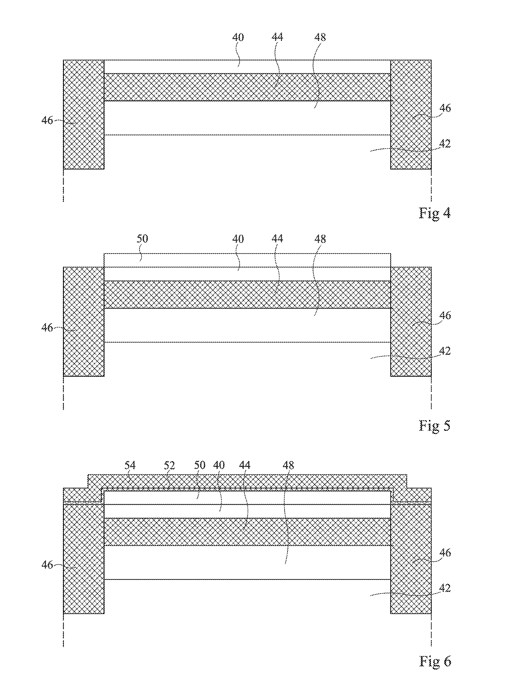
[0047]At a step illustrated in FIG. 4, a dopant implantation has been pe...


PUM

PropertyMeasurementUnit
thicknessaaaaaaaaaa
thicknessaaaaaaaaaa
thicknessaaaaaaaaaa

Abstract

A method for manufacturing a bipolar transistor, including the steps of: forming a first surface-doped region of a semiconductor substrate having a semiconductor layer extending thereon with an interposed first insulating layer; forming, at the surface of the device, a stack of a silicon layer and of a second insulating layer; defining a trench crossing the stack and the semiconductor layer opposite to the first doped region, and then an opening in the exposed region of the first insulating layer; forming a single-crystal silicon region in the opening; forming a silicon-germanium region at the surface of single-crystal silicon region, in contact with the remaining regions of the semiconductor layer and of the silicon layer; and forming a second doped region at least in the remaining space of the trench.

Description

BACKGROUND[0001]1. Technical Field[0002]The present disclosure relates to bipolar transistors formed on an integrated circuit. More specifically, the present disclosure relates to a method for manufacturing such a transistor.[0003]2. Description of the Related Art[0004]In integrated circuits, it may be advantageous to integrate, on a same wafer, MOS transistors and bipolar transistors (integration better known as “BiCMOS”). Indeed, these two types of transistors have specific advantages. In particular, MOS transistors allow fast switchings for digital processings, while bipolar transistors have a particularly good performance at high frequencies, for example, higher than some hundred GHz, and may have a high output power. Thus, these last transistors may be used to form circuits for controlling optical circuits, for example, lasers.[0005]Thus, methods for simultaneously manufacturing MOS transistors and bipolar transistors on a same substrate are needed.[0006]FIG. 1 illustrates an e...

Claims


Application Information

Patent Timeline
Patent Type & Authority Applications(United States)
IPC IPC(8): H01L29/73H01L27/12H01L29/66
CPCH01L29/73H01L29/66234H01L27/1203H01L29/66242H01L29/66265H01L29/7317H01L29/7322H01L29/7371H01L29/1004H01L21/8249H01L29/66272
Inventor CHANTRE, ALAINCHEVALIER, PASCALAVENIER, GREGORY
Owner STMICROELECTRONICS SRL
Why Eureka
Try Eureka