Charged particle beam device and method of manufacture of sample

Inactive Publication Date: 2013-10-24
HITACHI HIGH-TECH CORP
View PDF17 Cites 14 Cited by
  • Summary
  • Abstract
  • Description
  • Claims
  • Application Information

AI Technical Summary

Benefits of technology

[0013]According to the present invention, an end-point moment of removal machining of a damaged layer can be automatically detected. Thus, a failure of the removal mach

Problems solved by technology

However, in the machining with a FIB machining device, an ion penetrates into the inside of the sample.
For example, when the sample has a crystal structure, there is such a problem that the crystal structure is broken by irradiation of the ions to cr

Method used


Image

  • Charged particle beam device and method of manufacture of sample
  • Charged particle beam device and method of manufacture of sample
  • Charged particle beam device and method of manufacture of sample

Examples


Example

[0026]Embodiments of the present invention will be described hereinafter based on the drawings. The embodiments of the present invention are incidentally not limited to an example of modes described below, but various modifications are possible within a scope of its technical concept.

Example of Modes

(1) Device Configuration

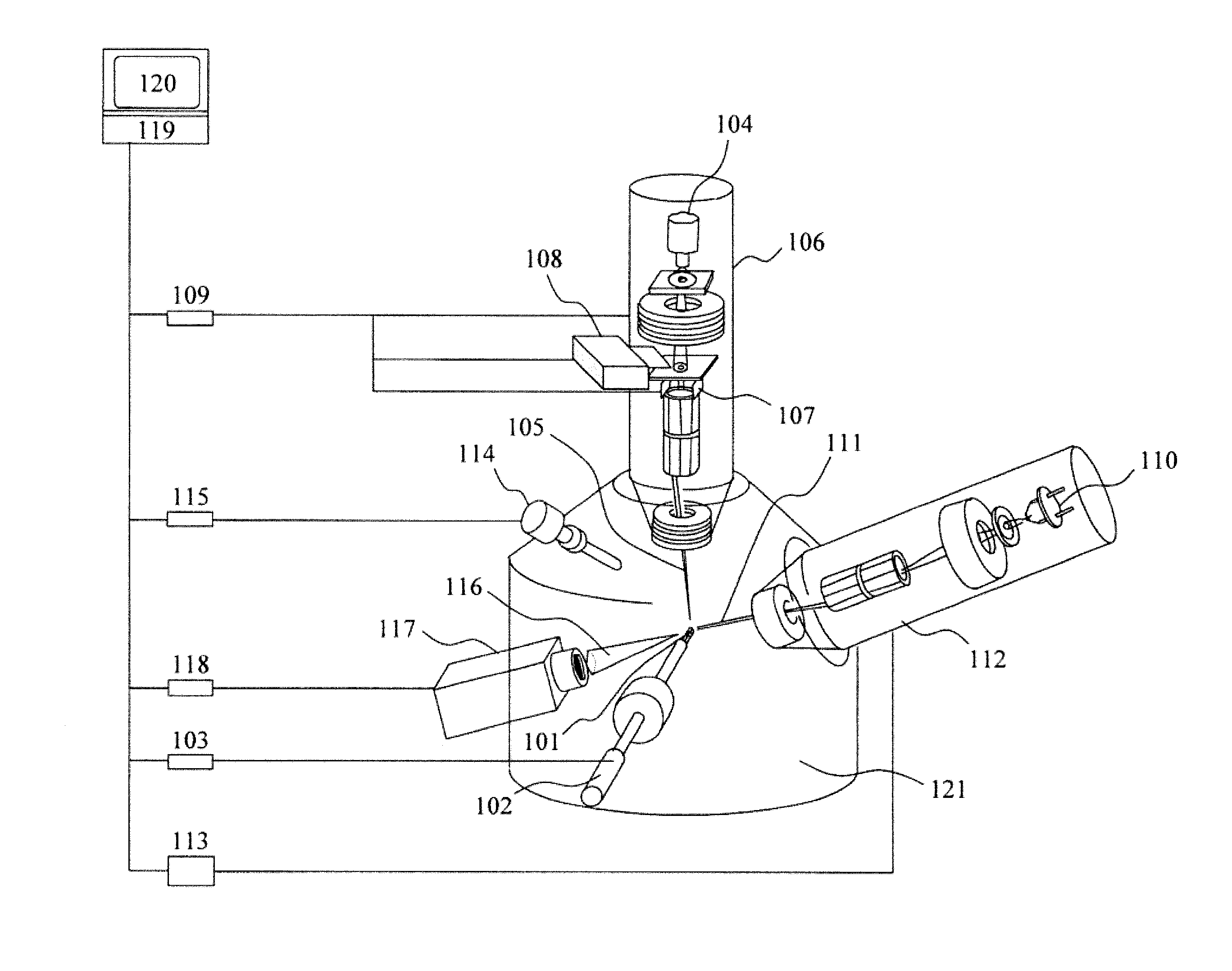
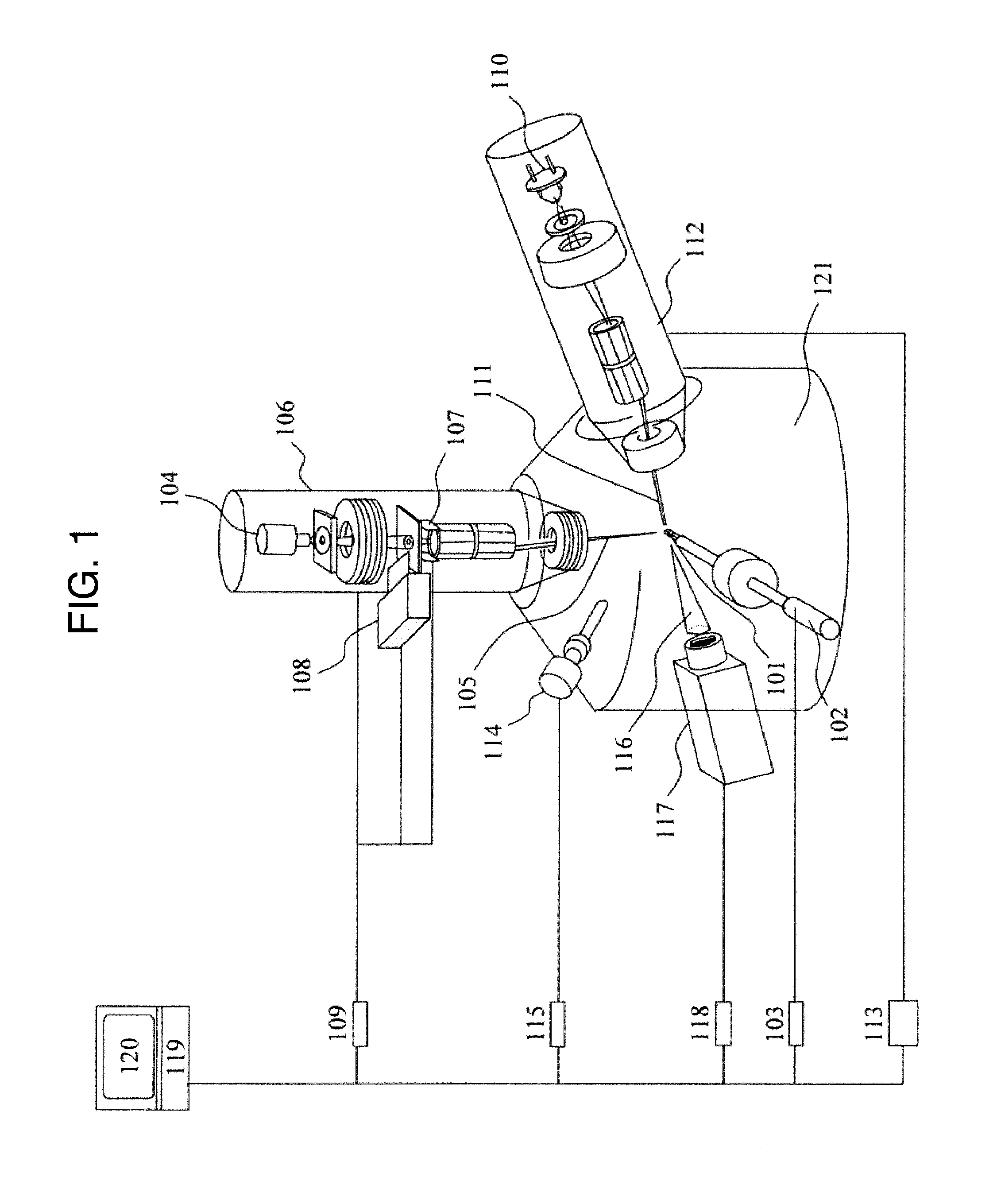
[0027]FIG. 1 shows a configuration diagram of a charged particle beam device. The charged particle beam device has: a movable sample stage 102 on which a sample 101 is mounted; a sample position control unit 103; an ion beam optics system apparatus 106; an ion beam optics system control unit 109; an electron beam optics system apparatus 112; an electron beam optics system control unit 113; a secondary electron detector 114; a secondary electron detector control unit 115; a two-dimensional detector 117; a two-dimensional detector control unit 118; a central processing unit 119; a display apparatus 120; and a vacuum container 121.

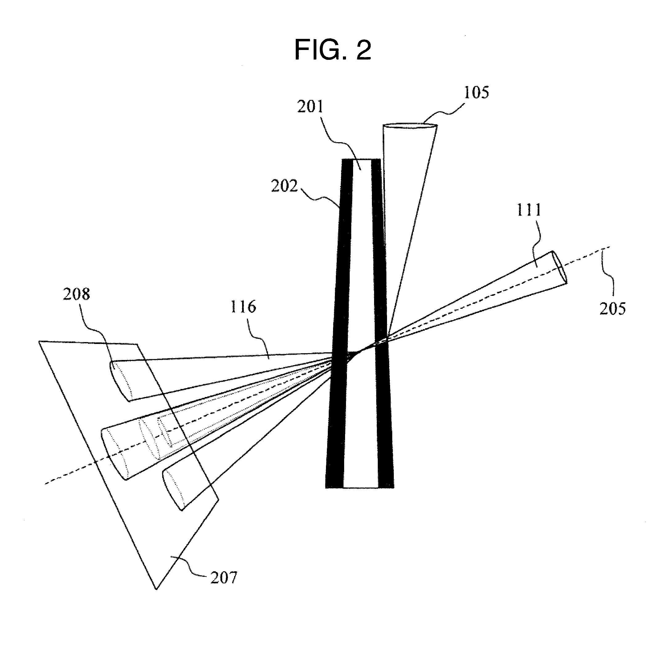
[0028]Here, the sample position cont...


PUM


Abstract

A precision of removal of a damaged layer of a sample created by machining with an FIB machining device depends on a skill of an operator. During removal machining of the damaged layer generated by an ion beam, transmitted electrons which are generated by irradiating an electron beam formed in an electron beam optics system onto a sample are detected by a two-dimensional detector, and a moment for finishing the removal machining of the damaged layer is determined based on the amount of blur of a diffraction pattern acquired with the two-dimensional detector.

Description

TECHNICAL FIELD[0001]The present invention relates to a charged particle beam device for machining a semiconductor device or the like for the purpose of an inspection and a defect analysis, and to a sample manufacturing method using such a device.BACKGROUND ART[0002]With miniaturization of a circuit pattern constructing a semiconductor device, inspection of an electronic defect and investigation of causes become important. Particularly, in order to investigate causes of generation of defects, importance of such a defect analysis, in which shapes and materials are analyzed while a sample is cut and machined, is increasing. When the miniaturization reaches a level of nanometers, an analysis with a Transmission Electron Microscope (hereinafter, referred to as a “TEM”) or a Scanning Transmission Electron Microscope (hereinafter, referred to as a “STEM”) is indispensable. In observations with these microscopes, a sample has to be cut and machined into a sample piece of proper dimensions....

Claims


Application Information

Patent Timeline
IPC IPC(8): H01J37/304
CPCH01J37/304H01J37/3056H01J2237/2804H01J2237/30466H01J2237/31749
Inventor NANRI, TERUTAKATOMIMATSU, SATOSHIAGEMURA, TOSHIHIDE
Owner HITACHI HIGH-TECH CORP
Why Eureka
Try Eureka