

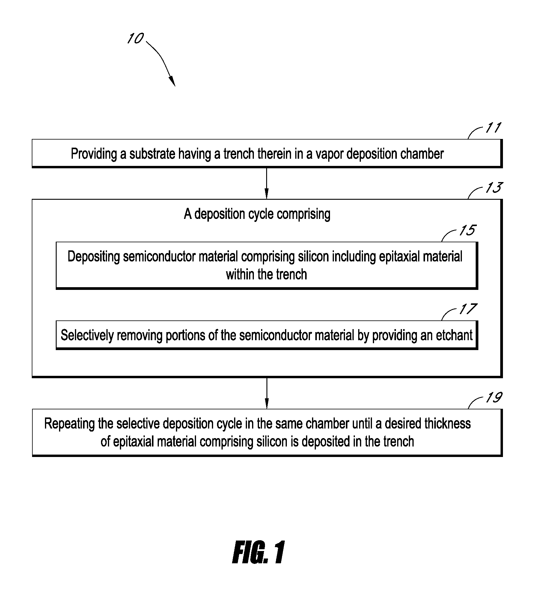
Processes and structures for dopant profile control in epitaxial trench fill
a technology of profile control and trench filling, which is applied in the direction of basic electric elements, electrical apparatus, semiconductor devices, etc., can solve the problems of non-uniform composition of trench-fill epitaxial materials
- Summary
- Abstract
- Description
- Claims
- Application Information
AI Technical Summary
Benefits of technology
Problems solved by technology
Method used
Image

Examples
example 1
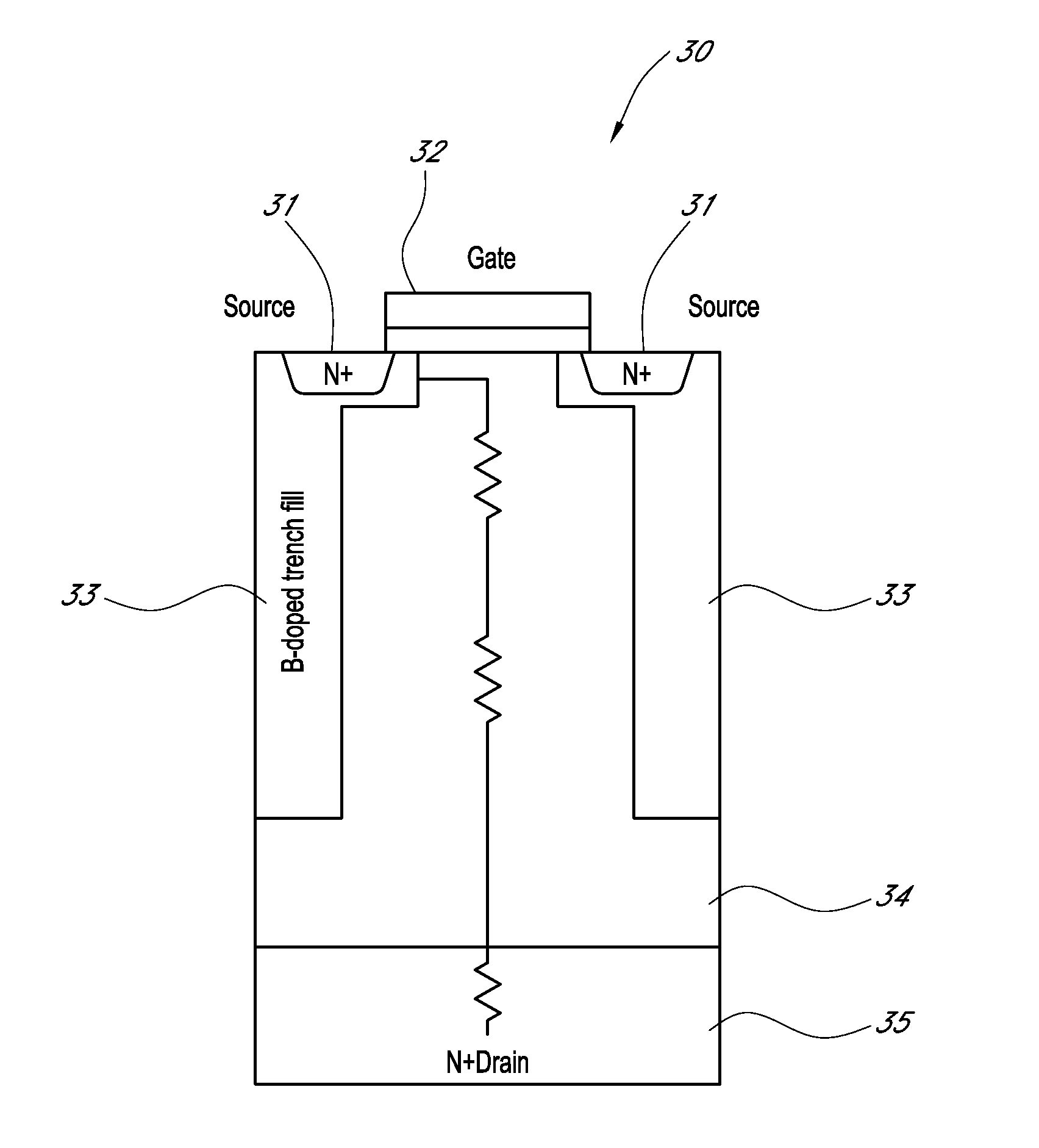
[0066]A substrate is first provided with a trench having a width of 4-5 μm and a height of about 50 μm. An epitaxial carbon and silicon trench liner is first deposited using MMS. Boron and germanium sources are not provided during deposition of the trench liner. The liner is deposited to a thickness of about 1000 Å over the walls and bottom of the recess.
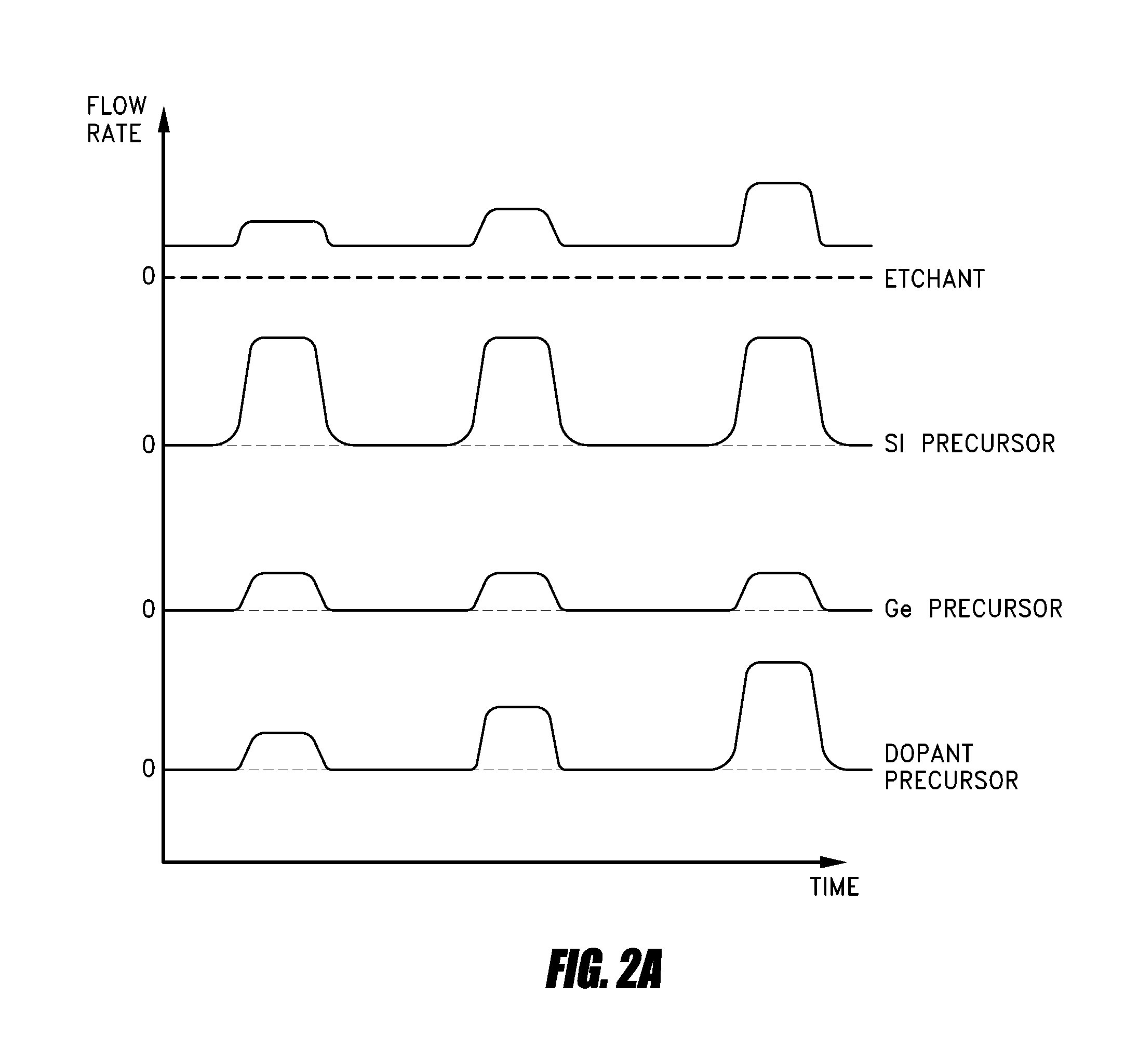
[0067]The trench is then filled by deposition of a boron and germanium doped silicon film using CDE. The boron source is diborane, the germanium source is germane (GeH4), and dichlorosilane is used as the silicon source. HCl is provided continuously during the cycle, but not at a constant rate. In each cycle, the boron, silicon, and germanium sources are first provided with the HCl followed by just providing HCl. The flow rates of HCl and diborane are both increased in each successive cycle such that the boron concentration in the deposited film is substantially the same as the concentration deposited in the previous cycle. The boro...
PUM
 Abstract
Description
Claims
Application Information