Electron Microscope and Method of Operating the Same

a technology of electron microscope and electron microscope, which is applied in the field of electron microscope, can solve the problems of inability to remove or re-add appropriate brightness, impaired ability to remove emission noise, and problems, and achieve the effect of suppressing the variation in the results of the calculation of effective valu

Active Publication Date: 2013-12-12
JEOL LTD
View PDF1 Cites 10 Cited by
  • Summary
  • Abstract
  • Description
  • Claims
  • Application Information

AI Technical Summary

Benefits of technology

[0027]According to the electron microscope associated with the present invention, the ratio of the amount of the electron beam detected by the electron beam detecting portion to the magnitude of the signal obtained by impingement of the electron beam on the sample varies according to various settings of the illumination system, imaging system, and detection system. Therefore, the DC component obtained as a result of the division performed by the division portion is varied. The signal indicative of the result of the division is multiplied by the DC component of the output signal from the electron beam detecting portion by the multiplication portion. Thus, the fluctuation portion can be compensated for. As a result, even when a noise canceling function is used, a noise-canceled image can be obtained by providing control similar to control provided where the noise canceling function is not used. During use, neither the contrast nor the brightness needs to be varied by switchingly enabling and disabling the noise canceling function.
[0028]Accordingly, the electron microscope associated with the present invention can achieve a noise cancellation method that can be adjusted more easily than the conventional analog division technique without being affected by decreases in emission current.
[0032]According to this electron microscope, by appropriately setting the given period of time, variations in the results of the calculation of the effective value can be suppressed if relatively low frequency AC components are contained in the output signal from the electron beam detecting portion.
[0033](4) An additional electron microscope associated with the present invention is based on the electron microscope (1) above and further characterized in that the DC component extracting portion may integrate an output signal from the electron beam detecting portion, remove DC components of the integral output signal to thereby produce a second integral signal, produce a third integral signal opposite in polarity to the second integral signal, and sum up the second and third integral signals.

Problems solved by technology

Therefore, appropriate brightness cannot be removed or re-added unless the factor Gn is controlled appropriately.
In addition to difficulties with adjustments, other problems occur.
Conversely, if 1 / (Gn×I2) is much smaller than 1, the ability to remove the emission noise will be impaired.

Method used


Image

  • Electron Microscope and Method of Operating the Same
  • Electron Microscope and Method of Operating the Same
  • Electron Microscope and Method of Operating the Same

Examples


first embodiment

1. First Embodiment

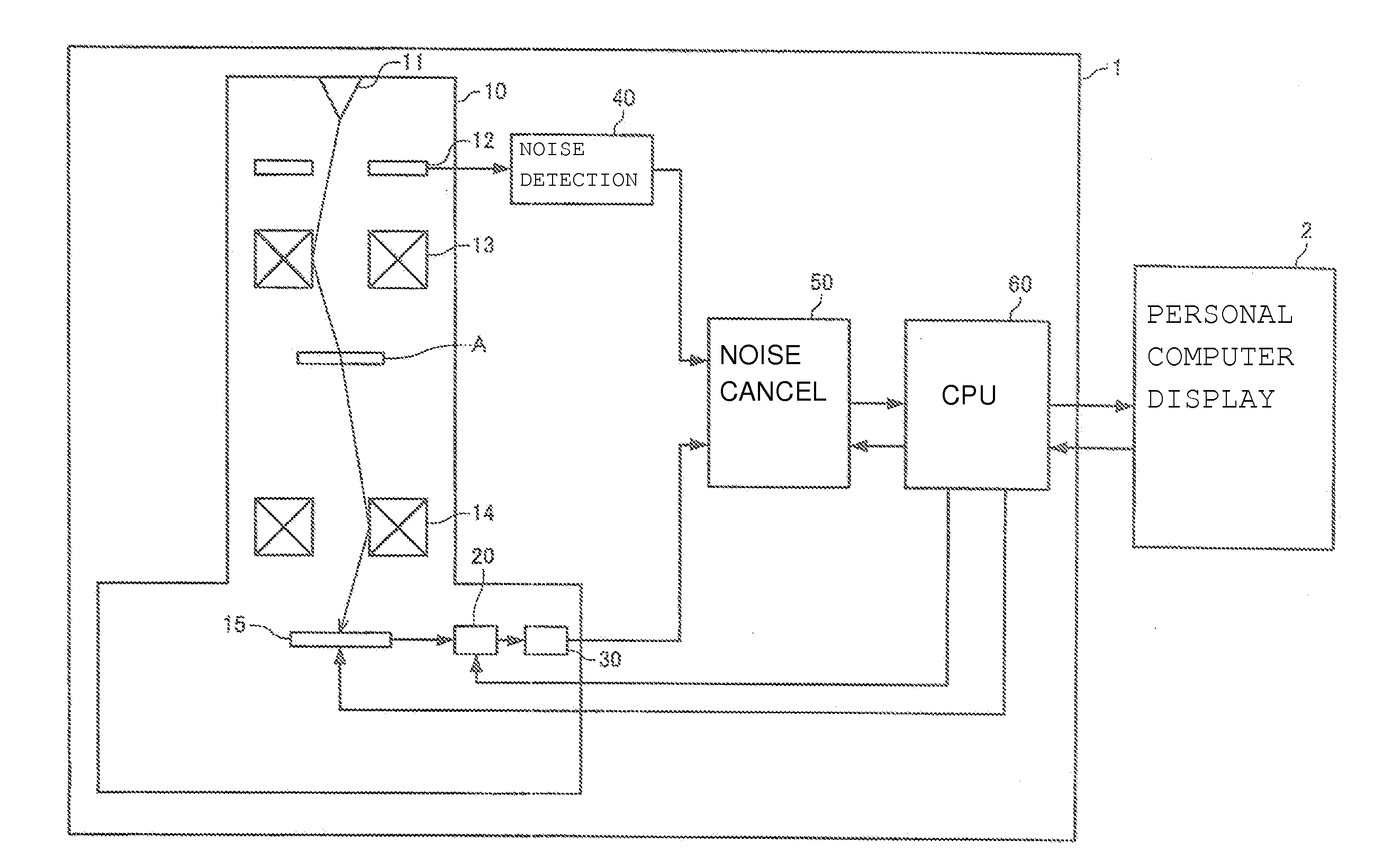
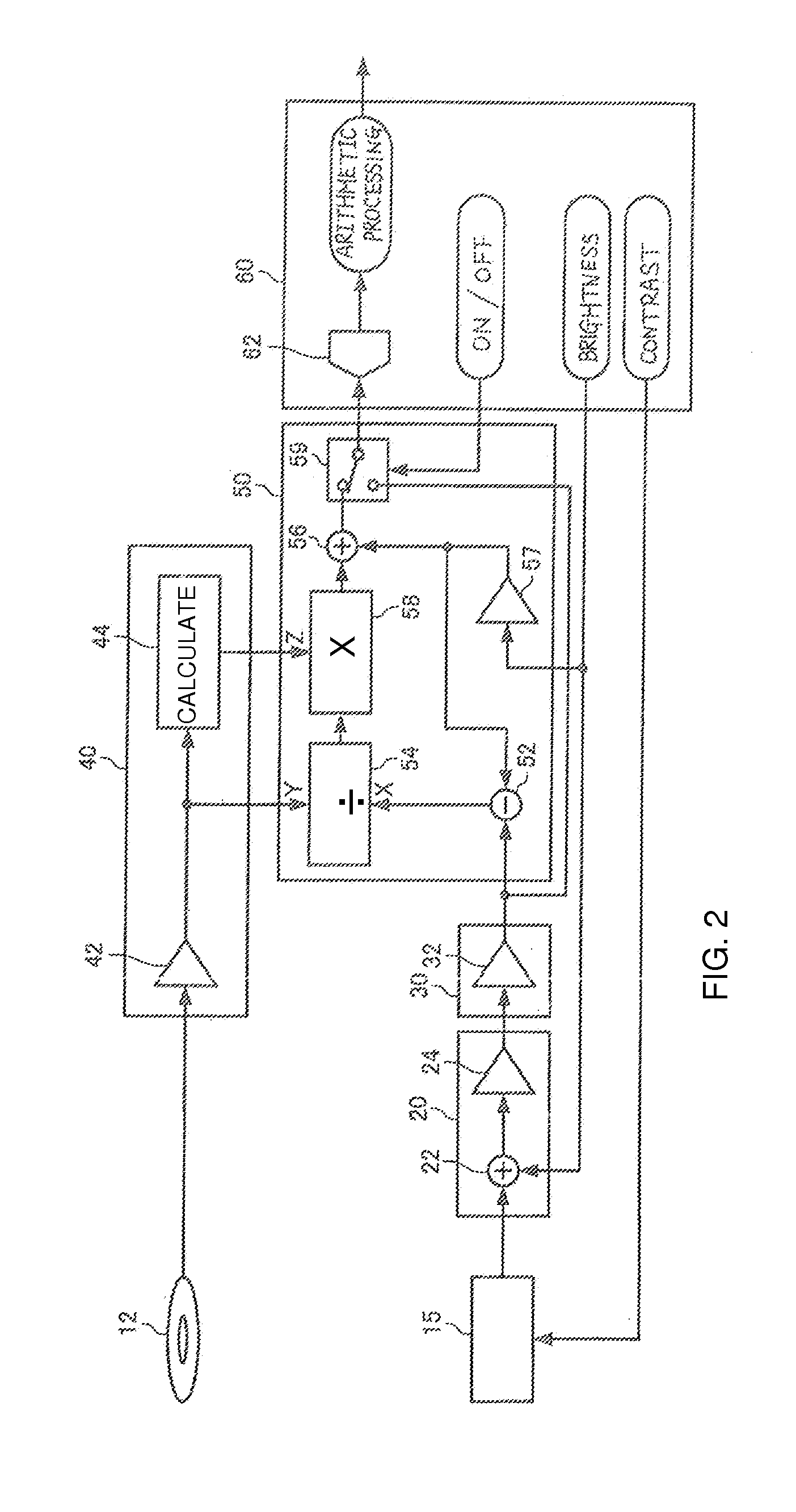
[0056]FIG. 1 shows one example of configuration of an electron microscope according to a first embodiment of the present invention. This microscope is generally indicated by reference numeral 1 and configured including an electron optical column 10, a noise detecting circuit 40, a noise canceling circuit 50, and a processing section (CPU) 60. An electron beam source 11, a noise canceling aperture 12, lenses 13, 14, a detector 15, a preamplifier circuit 20, an amplifier circuit 30, and other components are housed in the electron optical column 10. The electron microscope 1 is a scanning transmission electron microscope (STEM). Other types of lenses and apertures (not shown) are housed in the column 10. Some of the constituent elements of the electron microscope 1 of the present embodiment shown in FIG. 1 may be omitted, some modifications may be made to the constituent elements, or other constituent elements may be added.

[0057]The electron beam released from the el...

second embodiment

2. Second Embodiment

[0089]FIG. 5 is a diagram showing one example of configuration of an electron microscope according to a second embodiment of the present invention. FIG. 6 is a diagram showing one specific example of configuration of signal processing circuitry included in the microscope shown in FIG. 5. In FIGS. 5 and 6, the constituent elements which are the same as their counterparts shown in FIGS. 1 and 2 are indicated by the same reference numerals as in FIGS. 1 and 2 and their description is omitted. As shown in FIGS. 5 and 6, the electron microscope 1 of the second embodiment is similar to the electron microscope 1 of the first embodiment shown in FIGS. 1 and 2 except that the effective value calculating circuit 44 and the noise canceling circuit 50 are omitted and that the processing section 60 implements a noise canceling function (i.e., calculation of an effective value, subtraction of an offset value, division, multiplication, and addition of an offset value) by digita...

third embodiment

3. Third Embodiment

[0093]FIG. 7 is a diagram showing a specific example of configuration of signal processing circuitry in a third embodiment of the present invention. In both FIGS. 2 and 7, like constituent components are indicated by like reference numerals and their description is omitted. An electron microscope according to the third embodiment is similar in configuration with the microscope of FIG. 1 and so the microscope according to the third embodiment is neither illustrated nor described. As shown in FIG. 7, an electron microscope according to the third embodiment is similar in configuration with the electron microscope or the first embodiment shown in FIG. 2 except that the effective value calculating circuit 44 has been replaced by a filter circuit 70. The filter circuit 70 removes AC components from a noise signal amplified by a factor of Gn by the amplifier 42 and extracts DC components.

[0094]FIG. 8 is a diagram showing one example of configuration of the filter circuit...


PUM


Abstract

An electron microscope and method of operating an electron microscope (1) has an electron beam source (11) for producing an electron beam, a noise canceling aperture (12) for detecting a part of the beam, an amplifier (42), an effective value calculating circuit (44) for extracting DC components of the output signal from the amplifier (42), a detector (15) for detecting a signal obtained in response to impingement of the beam on a sample (A), a preamplifier circuit (20), an amplifier circuit (30), a dividing circuit (54) for performing a division based on the output signal from the amplifier circuit (30) and on the output signal from the amplifier (42), and a multiplier circuit (58) for performing multiplication of the output signal from the dividing circuit (54) and the output from the effective value calculating circuit (44).

Description

BACKGROUND OF THE INVENTION[0001]1. Field of the Invention[0002]The present invention relates to an electron microscope and method of operating it.[0003]2. Description of Related Art[0004]Generally, electrons released from a field-emission electron gun contain a fluctuation portion representing several percent of the total amount, because gas is adsorbed onto the emitter surface and adsorbed gas and ions migrate, varying the work function of the metal surface and because ion bombardment varies the metal surface morphology. Therefore, where a field-emission electron gun is used in a scanning transmission electron microscope (STEM), emission noise on the image is removed by placing a detector for noise cancellation in the electron optical column, detecting near electrons forming a probe to thereby form an electron signal, and dividing a signal released from the sample by the electron signal. This noise cancellation technique is disclosed, for example, in JP-A-5-307942.[0005]FIG. 13 sh...

Claims


Application Information

Patent Timeline
Patent Type & Authority Applications(United States)
IPC IPC(8): G06F17/18H01J37/285
CPCG06F17/18H01J37/285H01J37/28H01J2237/06341H01J2237/24495H01J2237/24507
Inventor SUZUKI, TAKASHI
Owner JEOL LTD
Why Eureka
Try Eureka