Semi-automated method of FPGA timing closure

a timing closure and semi-automatic technology, applied in the field of semi-automatic fpga timing closure, can solve the problems of slow and inefficient existing timing closure methods, and is not suitable for many ic design processes

US20130339913A1Inactive Publication Date: 2013-12-19STAVINOV EVGENI
1 Cites 3 Cited by

Patent Information

Authority / Receiving Office
US · United States
Current Assignee / Owner
Publication Date
2013-12-19
Estimated Expiration
Not applicable · inactive patent

Smart Images

  • Figure 1
    Figure 1
  • Figure 2
    Figure 2
  • Figure 3
    Figure 3
Patent Text Reader

Abstract

The invention describes a semi-automated method and system for Field Programmable Gate Array (FPGA) timing closure. The method is used to achieve timing closure by storing all previous results of design synthesis, place & route, tool options, and area constraints in a database, applying a set of analysis algorithms on the entire build history, and applying a decision engine to determine set of synthesis and place & route tool options and area constraints for the next build iteration. The aim of the inventive method is to eliminate most of the manual steps during design timing closure. The inventive method further makes the process faster, requiring fewer build iterations, and more robust to small design changes that can affect timing results. The desired outcome is achieved by making decisions based on the analysis of all the previous build results.
Need to check novelty before this filing date? Find Prior Art

Description

FIELD OF THE INVENTION

[0001] The invention in general is related to electronic circuit timing closure and in particular to the semi-automated FPGA timing closure method.BACKGROUND OF THE INVENTION

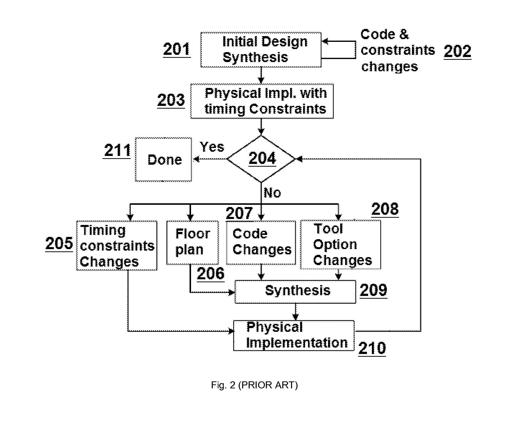
[0002] Several types of Integrated Circuits (IC) are used in numerous electronic equipments today. The Field-Programmable Gate Array (FPGA) is a type of Integrated Circuits which is configurable by a customer. In a standard circuit design flow, timing closure relates to the ability to design a system or module that meets certain speed expectations without flaws being experienced in the behavior of the system. This means that a circuit designer can test a circuit during the design process to ensure that timing violations do not affect the operation of the circuit. An FPGA build process refers to a sequence of steps to build an FPGA design from a generic RTL design description and design constraints to a bit stream. The exact build sequence will differ, depending on the FPGA vendor. A typical F...

Examples

Embodiment Construction

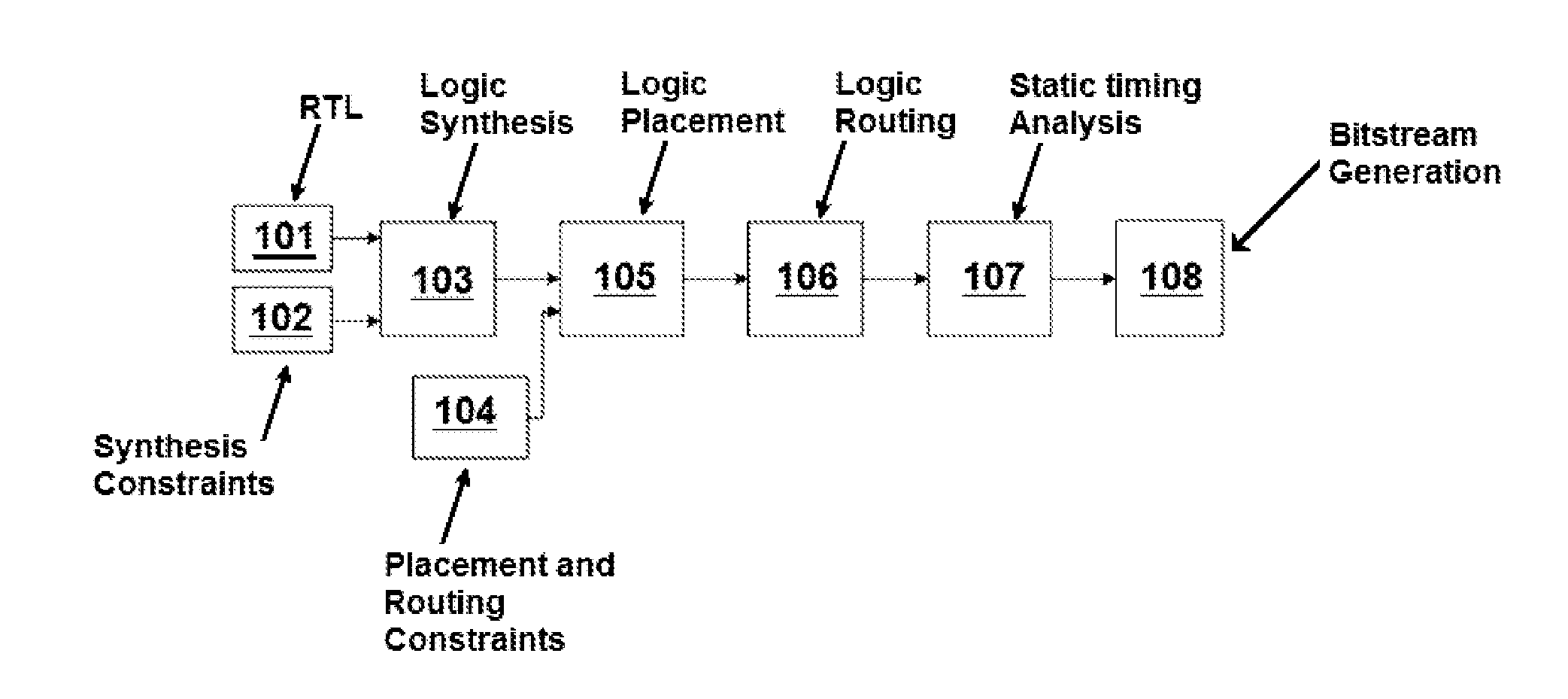
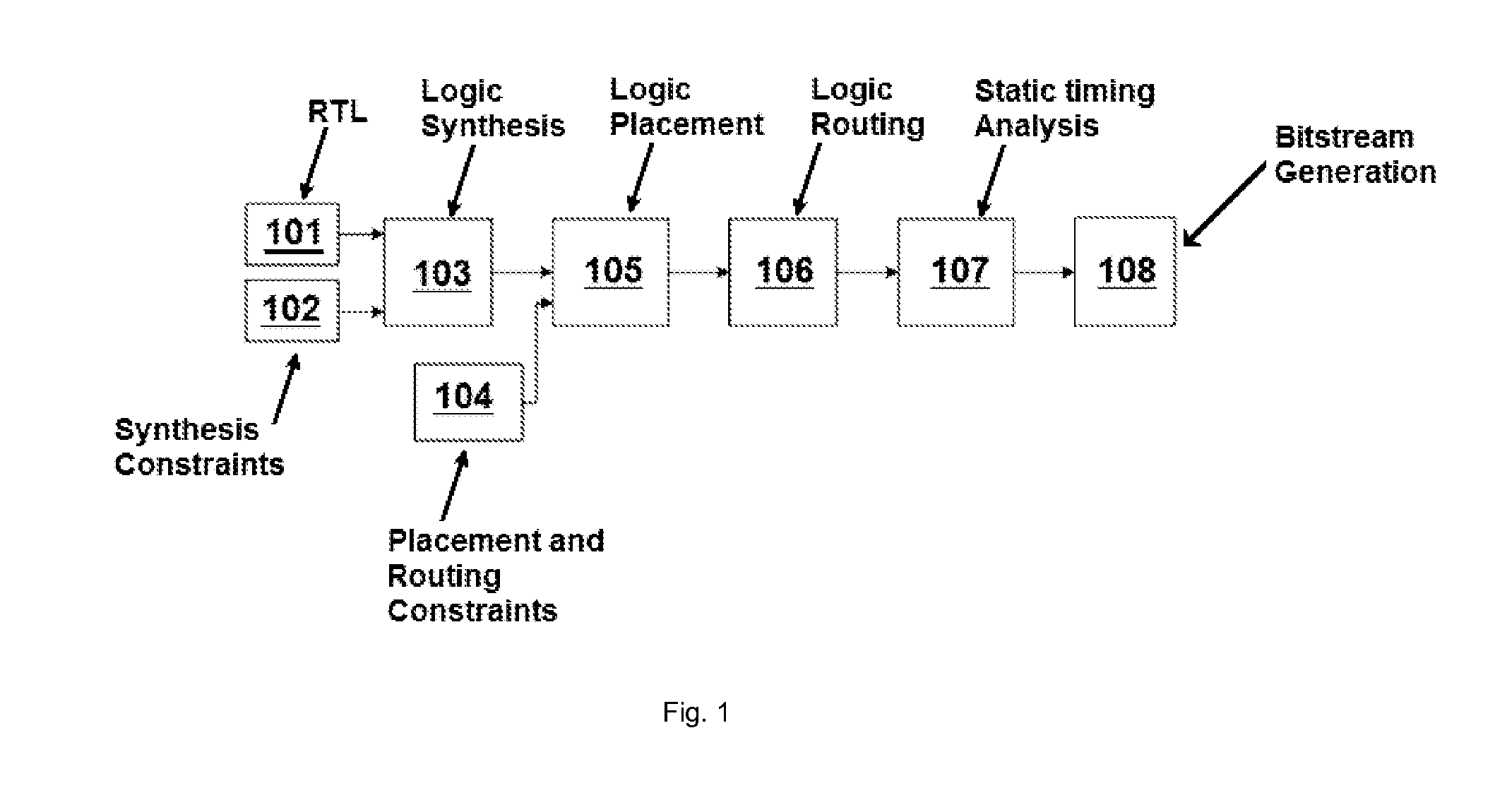
[0012]FIG. 1 shows a process of FPGA building as a sequence of steps carried out in the building of an FPGA circuit from a Register Transfer Level (RTL). A typical process of FPGA building includes an RTL 101, which is a level of abstraction used in describing the operation of a synchronous digital circuit. Another input apart from the RTL, is a set of synthesis constraints 102 that is fed into the logic of synthesis 103. In this process, placement and routing constraints play a major role in determining the actual floorplanning. In order to achieve a higher speed and timing closure, optimized routing and placement is necessary. Floorplanning a large, high speed design is the key to achieving timing closure. A good floorplanning can dramatically improve the design performance, and ensure consistent quality of the build results. Poor floorplanning can have an opposite effect, namely, making it impossible to meet timing constraints and cause inconsistent build results. Any of the floo...