Semiconductor device fabrication methods

a technology of semiconductor devices and fabrication methods, applied in semiconductor/solid-state device manufacturing, transistors, electric devices, etc., can solve the problems of increased process complexity and cost, increased cost, and inability to achieve salicide layer for passive devices

Inactive Publication Date: 2013-12-26
ALSEPHINA INNOVATIONS INC
View PDF14 Cites 4 Cited by
  • Summary
  • Abstract
  • Description
  • Claims
  • Application Information

AI Technical Summary

Benefits of technology

[0005]Semiconductor device fabrication methods are provided. In one embodiment, a method for fabricating a semiconductor device includes forming first and second gate structures overlying the semiconductor substrate, and depositing a layer of a silicide-resistant material over the first and second gate structures and over the semiconductor substrate. The method further includes forming sidewall spacers from the layer of silicide-resistant material adjacent the first gate structure and removing the silicide-resistant material adjacent the sidewall spacers to expose the silicon substrate in a source and drain region. Still further, the method includes implanting conductivity determining impurities in the source and drain region, depositing a silicide forming metal, and annealing the semiconductor device to form a silicide in the source and drain region. The silicide-resistant material is not removed from over the second gate structure so as to prevent silicide formation at the second gate structure.

Problems solved by technology

The use of MOS transistor devices for logic as well as memory applications, as well as for passive devices such as resistors, electrostatic-sensitive (ESD) devices, and laterally diffused metal oxide semiconductor (LDMOS) devices, all fabricated on the same semiconductor chip, has resulted in increased process complexity as well as increased cost.
For example, a self-aligned metal silicide (“salicide”) layer is often used with the high performance logic devices, while the salicide layer is not desired for passive devices.
The formation of a separate and dedicated silicide masking layer, along with its subsequent removal after silicidation is complete, adds multiple process steps to the semiconductor fabrication process, and consequently increases the cost thereof.
Further, the removal of the silicide masking layer requires the deposition of a photoresist material and etching, which can damage the MOS transistor devices when performed multiple times, especially in small-scale architectures such as 28 nm architectures.

Method used


Image

  • Semiconductor device fabrication methods
  • Semiconductor device fabrication methods
  • Semiconductor device fabrication methods

Examples


Embodiment Construction

[0010]The following detailed description is merely illustrative in nature and is not intended to limit the embodiments of the subject matter or the application and uses of such embodiments. As used herein, the word “exemplary” means “serving as an example, instance, or illustration.” Any implementation described herein as exemplary is not necessarily to be construed as preferred or advantageous over other implementations. Furthermore, there is no intention to be bound by any expressed or implied theory presented in the preceding technical field, background, brief summary or the following detailed description.

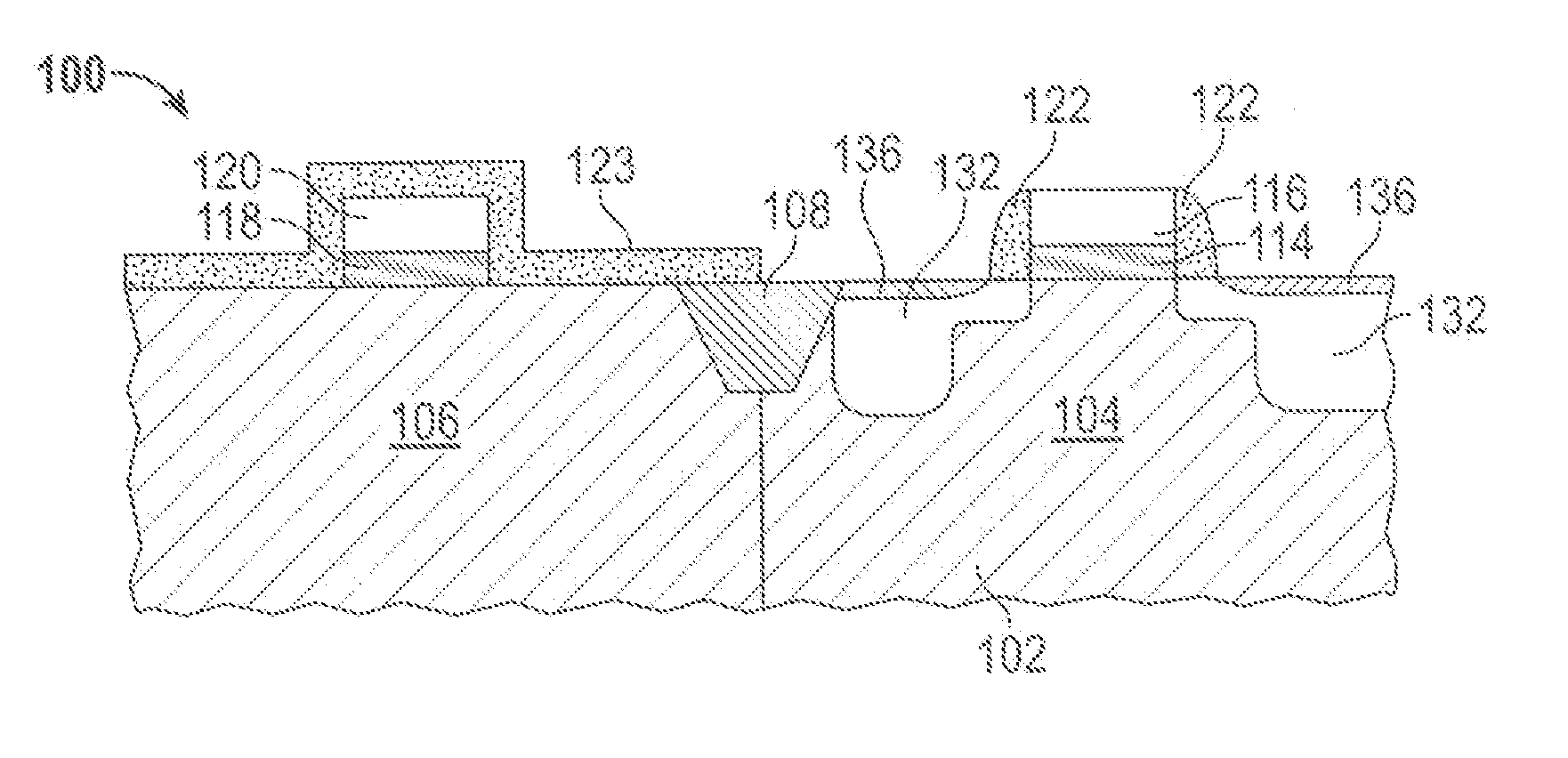
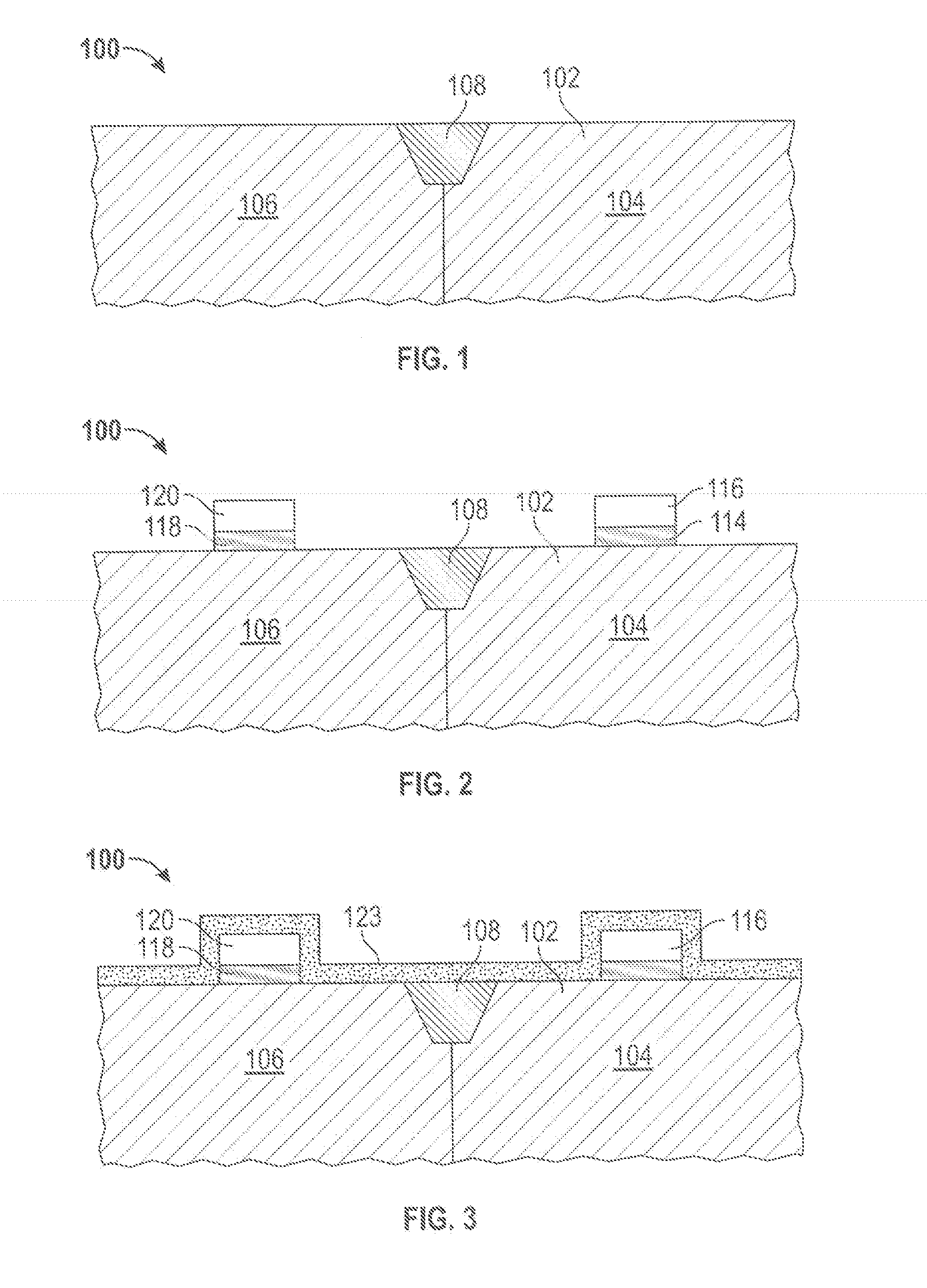
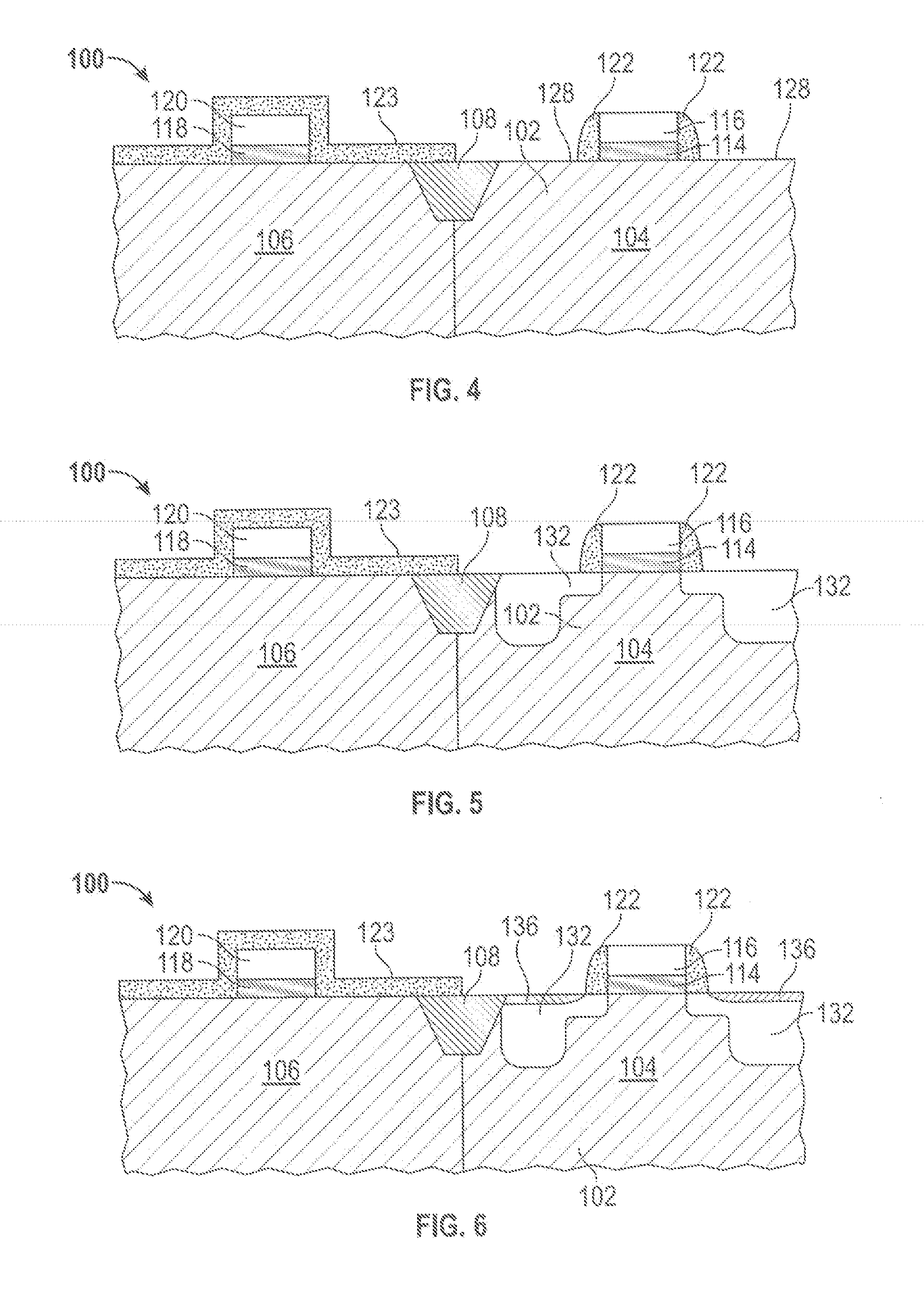
[0011]The techniques and technologies described herein may be utilized to fabricate MOS transistor devices. Although the term “MOS transistor device” properly refers to a device having a metal gate electrode and an oxide gate insulator, that term will be used throughout to refer to any semiconductor device that includes a conductive gate electrode (whether metal or other conduct...


PUM


Abstract

A method for fabricating a semiconductor device includes forming first and second gate structures overlying the semiconductor substrate, and depositing a layer of a silicide-resistant material over the first and second gate structures and over the semiconductor substrate. The method further includes forming sidewall spacers from the layer of silicide-resistant material adjacent the first gate structure and removing the silicide-resistant material adjacent the sidewall spacers to expose the silicon substrate in a source and drain region. Still further, the method includes implanting conductivity determining impurities in the source and drain region, depositing a silicide forming metal, and annealing the semiconductor device to form a silicide in the source and drain region. The silicide-resistant material is not removed from over the second gate structure so as to prevent silicide formation at the second gate structure.

Description

TECHNICAL FIELD[0001]Embodiments of the subject matter disclosed herein generally relate to semiconductor device fabrication methods, and more particularly, embodiments of the subject matter disclosed herein relate to semiconductor device fabrication methods employing the contemporaneous formation of gate sidewall spacers and a silicide masking layer.BACKGROUND[0002]Transistors, such as metal oxide semiconductor field-effect transistors (“MOSFETs” or “MOS” transistor devices), are the core building block of the vast majority of semiconductor devices. Some semiconductor devices, such as high performance processor devices, can include millions of transistors. For such devices, decreasing transistors size, and thus increasing transistor density, has traditionally been a high priority in the semiconductor manufacturing industry.[0003]The use of MOS transistor devices for logic as well as memory applications, as well as for passive devices such as resistors, electrostatic-sensitive (ESD)...

Claims


Application Information

Patent Timeline
Patent Type & Authority Applications(United States)
IPC IPC(8): H01L21/336H01L21/28
CPCH01L29/6659H01L21/823418H01L21/823443H01L29/7833
Inventor KURZ, ANDREASJAVORKA, PETERMUTAS, SERGEJWUNDISCH, CLEMENS
Owner ALSEPHINA INNOVATIONS INC
Why Eureka
Try Eureka