Method to increase charge retention of non-volatile memory manufactured in a single-gate logic process

a logic process and non-volatile memory technology, applied in the field of non-volatile memory, can solve the problems of difficult to fabricate both of these circuits on the same chip, high wafer price, and minor local degradation of gate dielectric quality, and achieve the effects of thinning or removing this structure, preventing the formation of silicide, and reducing the diffusion of metallic particles

Inactive Publication Date: 2007-07-26
MOSYS INC
View PDF59 Cites 11 Cited by
  • Summary
  • Abstract
  • Description
  • Claims
  • Application Information

AI Technical Summary

Benefits of technology

[0014] In accordance with another aspect of the invention, the silicide-blocking dielectric structure may be formed such that the silicide regions formed on the active regions of the NVM cell are separated from the edges of these active regions. This advantageously minimizes the diffusion of metallic particles from these silicide regions through the field dielectric.
[0015] In another embodiment of the present invention, the silicide-blocking dielectric structure is formed entirely over the NVM cell, thereby blocking silicide formation on the active regions of the NVM cell. After silicide formation has been performed for the logic devices, the silicide-blocking dielectric structure is etched, thereby thinning or removing this structure. A pre-metal dielectric layer is formed over the resulting structure, and a contact etch is performed to expose the active regions of the NVM cell and the silicided regions of the logic devices. Thinning (or removing) the silicide-blocking dielectric structure ensures that the contact etch associated with a conventional logic process will reliably expose the active regions of the NVM cell.

Problems solved by technology

The different requirements of traditional NVM circuits and logic circuits makes it difficult to fabricate both of these circuits on the same chip.
The combination of an NVM circuit and a conventional logic circuit therefore typically requires the use of a much more complicated and expensive “merged non-volatile memory and logic” process, and results in a high wafer price.
In general, silicide spiking events are rare and result in minor local degradation of gate dielectric quality or a small gate dielectric leakage increase for an entire chip that contains many millions of transistors.

Method used


Image

  • Method to increase charge retention of non-volatile memory manufactured in a single-gate logic process
  • Method to increase charge retention of non-volatile memory manufactured in a single-gate logic process
  • Method to increase charge retention of non-volatile memory manufactured in a single-gate logic process

Examples


Embodiment Construction

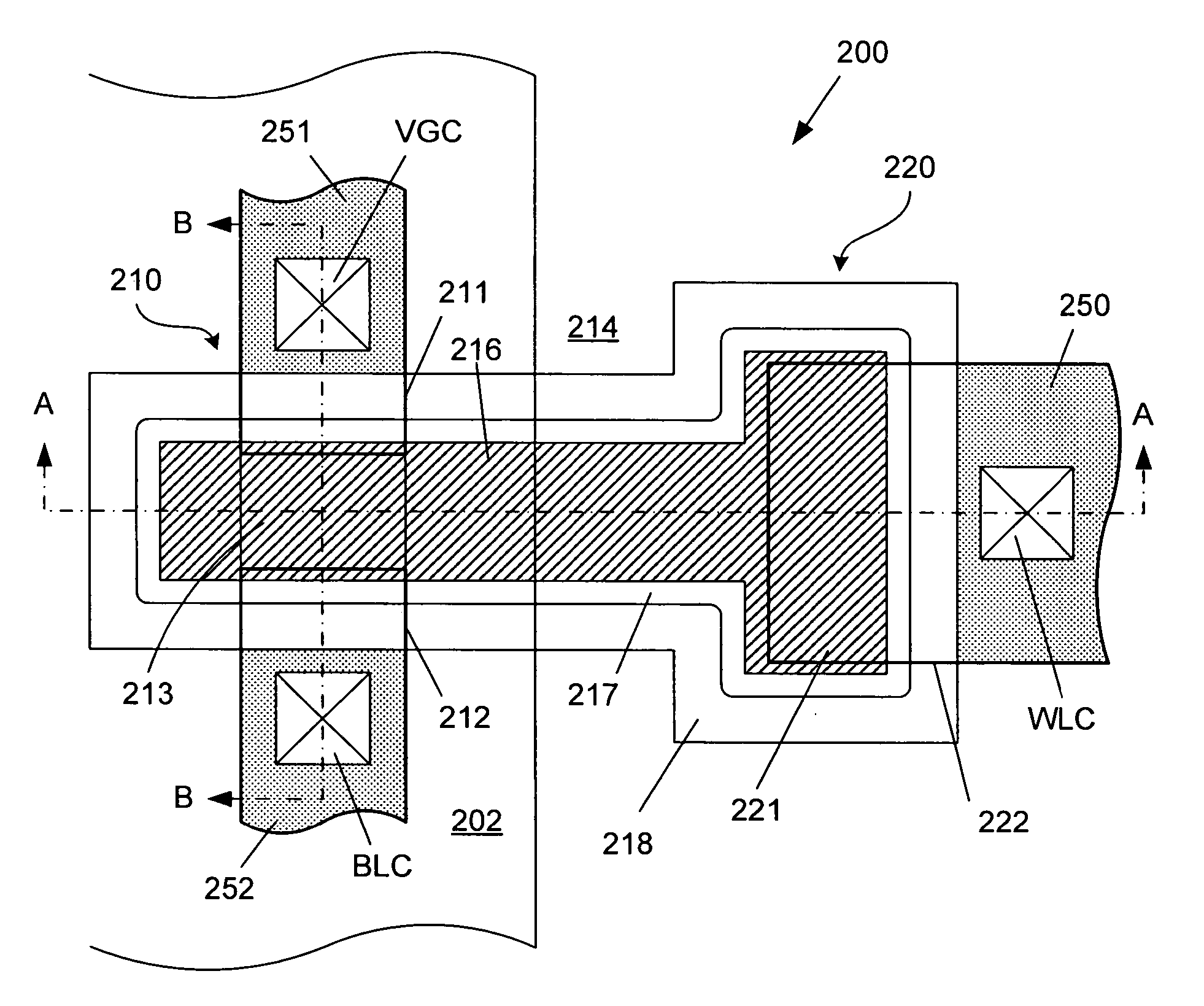
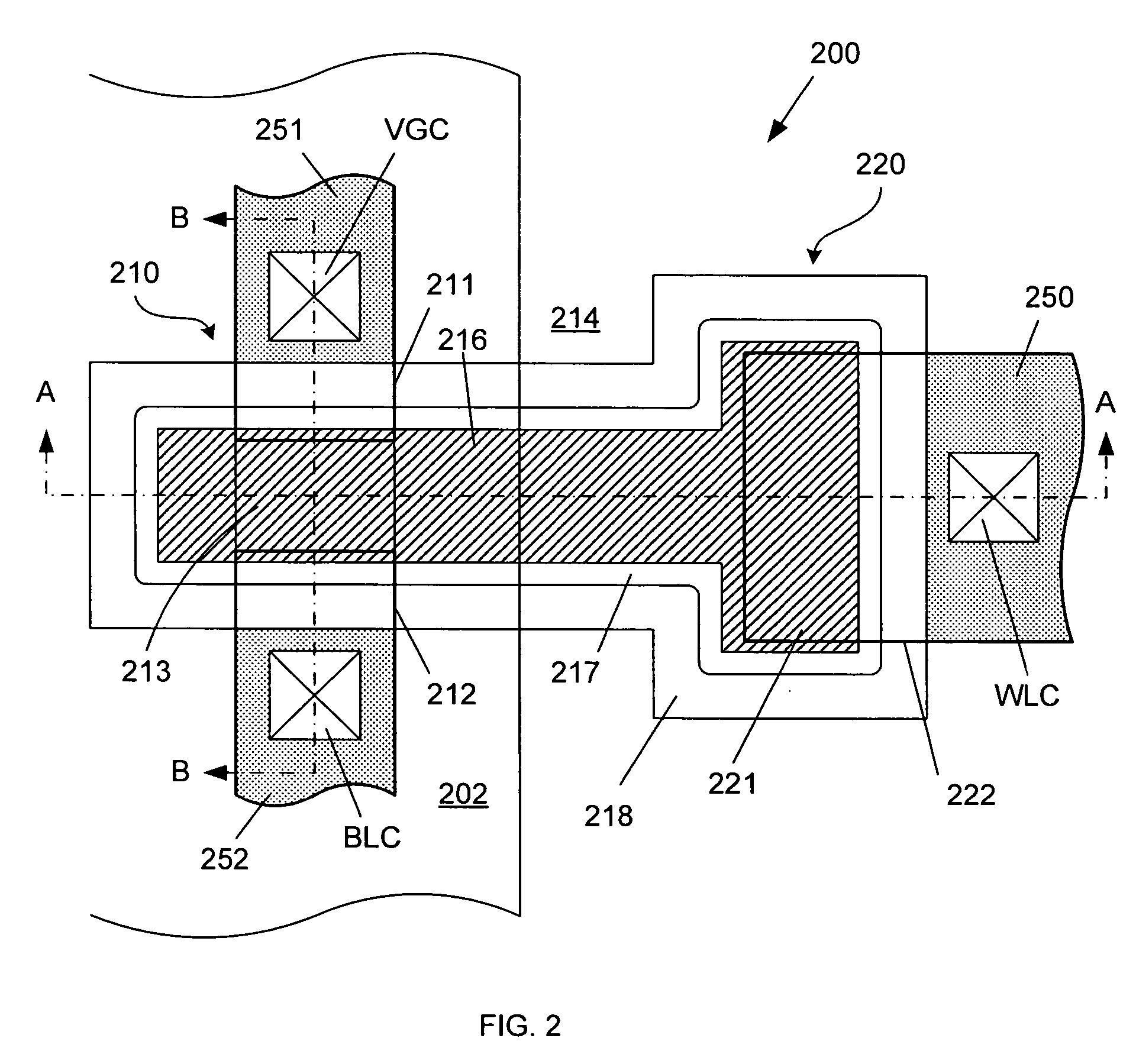
[0031]FIG. 2 is a top layout view of a non-volatile memory cell 200 in accordance with one embodiment of the present invention. FIG. 3A is a cross-sectional view of the non-volatile memory cell of FIG. 2 along section line A-A. FIG. 3B is a cross-sectional view of the non-volatile memory cell of FIG. 2 along section line B-B. Non-volatile memory cell 200 can be operated in response to a positive Vdd supply voltage and a Vss supply voltage of 0 Volts.

[0032] Note that the general layout of non-volatile memory cell 200 is similar to the layout of the NVM cell described in commonly owned U.S. Pat. No. 6,512,691 (hereinafter, the '691 Patent). The portions of the '691 Patent which describe the fabrication and operation of common elements in the NVM cell 200 of the present invention and the NVM cell of the '691 Patent are hereby incorporated by reference. Although the present invention is described using a specific NVM cell 200, it is understood that the present invention is in no way li...


PUM


Abstract

A non-volatile memory cell with increased charge retention is fabricated on the same substrate as logic devices using a single-gate conventional logic process. A silicide-blocking dielectric structure is formed over a floating gate of the NVM cell, thereby preventing silicide formation over the floating gate, while allowing silicide formation over the logic devices. Silicide spiking and bridging are prevented in the NVM cell, as silicide-blocking dielectric structure prevents silicide metal from coming in contact with the floating gate or adjacent sidewall spacers. The silicide-blocking dielectric layer may expose portions of the active regions of the NVM cell, away from the floating gate and adjacent sidewall spacers, thereby enabling silicide formation on these portions. Alternately, the silicide-blocking dielectric layer may cover the active regions of the NVM cell during silicide formation. In this case, silicide-blocking dielectric layer may be thinned or removed after silicide formation.

Description

FIELD OF THE INVENTION [0001] The present invention relates to non-volatile memory (NVM). More particularly, this invention relates to non-volatile memory cells fabricated using an ASIC or conventional logic process. In the present application, a conventional logic process is defined as a semiconductor process that implements single-well or twin-well technology and uses a single gate layer. This invention further relates to a method of operating a non-volatile memory to ensure maximum data retention time. BACKGROUND OF INVENTION [0002] Many modern integrated circuit applications demand the integration of non-volatile memory (NVM) and logic circuits on the same chip. However, traditional NVM cells are typically fabricated using a stacked gate structure or a split gate structure. Therefore, a typical NVM fabrication process requires the deposition of more than one gate layer. In contrast, logic circuits are typically fabricated using a semiconductor integrated circuit manufacturing pr...

Claims


Application Information

Patent Timeline
Patent Type & Authority Applications(United States)
IPC IPC(8): H01L29/76
CPCH01L21/28273H01L27/115H01L29/7883H01L29/42324H01L27/11521H01L29/40114H10B69/00H10B41/30
Inventor FANG, GANG-FENGSINITSKY, DENNISLEUNG, WINGYU
Owner MOSYS INC
Why Eureka
Try Eureka