Selective salicidation methods

a technology of selective salicidation and salicidation method, which is applied in the direction of basic electric elements, electrical equipment, semiconductor devices, etc., can solve the problems of limiting applicability, complex process, and many steps in the process, so as to prevent silicide formation and prevent silicide formation

a technology of selective salicidation and salicidation method, which is applied in the direction of basic electric elements, electrical equipment, semiconductor devices, etc., can solve the problems of limiting applicability, complex process, and many steps in the process, so as to prevent silicide formation and prevent silicide formation

US20050282370A1Inactive Publication Date: 2005-12-22IBM CORP

Image

  • Selective salicidation methods
  • Selective salicidation methods
  • Selective salicidation methods

Examples


Embodiment Construction

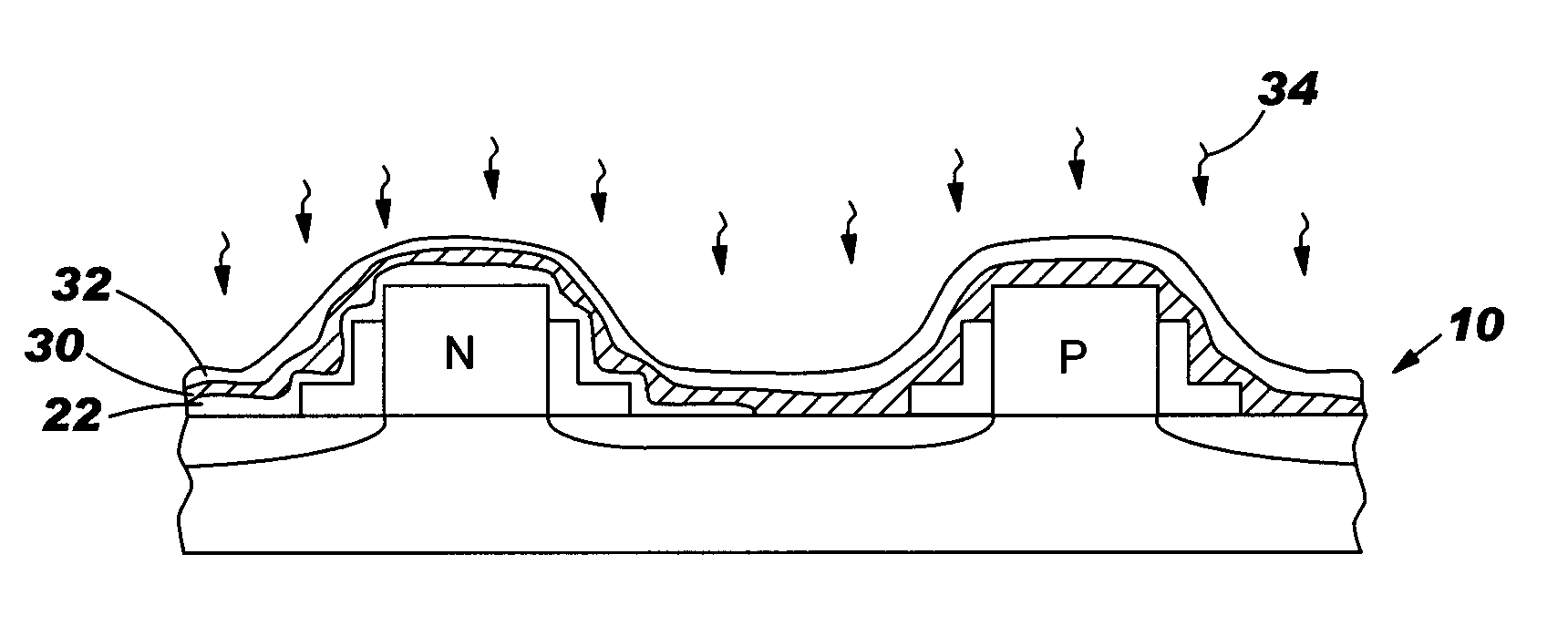
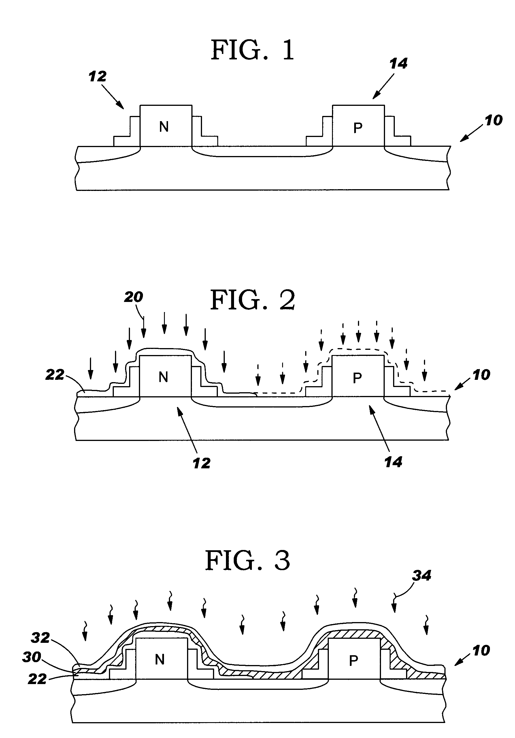
[0017] With reference to the accompanying drawings, FIGS. 1-4 illustrate a method for selective salicidation of a semiconductor device 10. As shown in FIG. 1, a first step includes forming (or providing) a first structure 12 having an n-type dopant at the surface in a p-type well, and a second structure 14 having a p-type dopant at the surface in a n-type well. The n-type dopant may include, for example, phosphorous and / or arsenic, and the p-type dopant may include, for example, boron and / or boron di-flouride. In one embodiment, first structure 12 is an n-type field effect transistor (NFET) 12 and second structure 14 is a p-type FET (PFET). It should be recognized, however, that structures 12, 14 may be any type of doped structure upon which selective salicidation is desired. First and second structure 12, 14 may be formed by any now known or later developed processing. For example, formation of the actual structures 12, 14, and then doping by implanting the particular dopants. In t...


PUM

PropertyMeasurementUnit
thicknessaaaaaaaaaa
temperatureaaaaaaaaaa
sheet resistanceaaaaaaaaaa

Abstract

Methods for selective salicidation of a semiconductor device. The invention implements a chemical surface pretreatment by immersion in ozonated water H2O prior to metal deposition. The pretreatment forms an interfacial layer that prevents salicidation over an n-type structure. As a result, the invention does not add any additional process steps to the conventional salicidation processing.

Description

BACKGROUND OF INVENTION [0001] 1. Technical Field [0002] The present invention relates generally to complementary metal-oxide semiconductor (CMOS) chip manufacturing, and in particular, to the process area for forming ohmic contacts to devices using self-aligning silicide (salicide) processing. [0003] 2. Related Art [0004] Formation of ohmic contacts to devices using self-aligning silicide (silicide) processing is a common semiconductor fabrication step. During this process, it is oftentimes advantageous to form silicide a p-type structure such as a field effect transistor (PFET), and not an n-type structure such as an NFET. Typically, however, selectively siliciding p+ silicon (Si) material requires additional blocking photomask levels, which adds many steps to the process and thus adds complexity. [0005] In one approach, disclosed in U.S. Pat. No. 5,342,798 to Huang, selective salicidation of source / drain regions of a transistor is performed by implanting into a first set of sourc...

Claims


Application Information

Patent Timeline
22 Dec 2005
Publication
US20050282370A1
IPC
H01L21/285; H01L21/3205; H01L21/336; H01L21/4763; H01L21/8238
CPC
H01L21/28518; H01L29/665; H01L21/823835
Inventors
ARNDT, RUSSELL H.; GIEWONT, KENNETH J.