
Method of etching silicon nitride films

a technology of silicon nitride and film, which is applied in the field ofplasma etching method of silicon nitride (sin) film, can solve the problem of limited etching of deep features on a wafer, and achieve good etch selectivity

Inactive Publication Date: 2013-12-26
TOKYO ELECTRON LTD
View PDF8 Cites 18 Cited by
  • Summary
  • Abstract
  • Description
  • Claims
  • Application Information

AI Technical Summary

Benefits of technology

The invention provides methods for making deep obstacles in SiN films using plasma etching. These methods can create straight sides and are very effective at removing the mask pattern and other materials.

Problems solved by technology

Therefore, etching of deep features on a wafer can be limited by the etch selectivity between the material of the mask pattern and the material to be etched, where the higher the selectivity, the deeper the feature may be etched.

Method used


Image

  • Method of etching silicon nitride films
  • Method of etching silicon nitride films
  • Method of etching silicon nitride films

Examples


Embodiment Construction

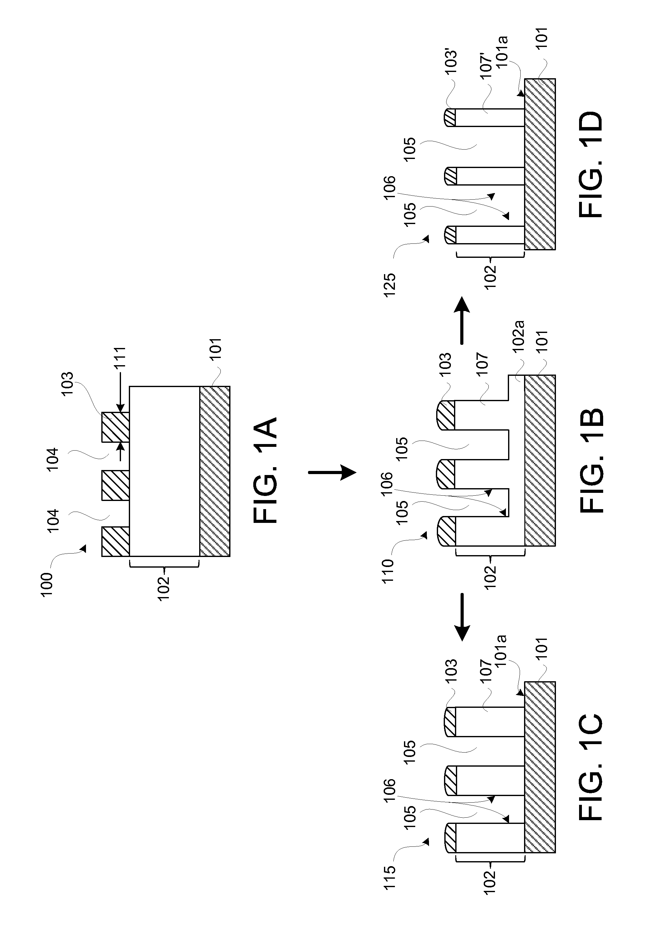
[0019]Embodiments of the invention are described with reference to the accompanying drawings, in which exemplary embodiments of the invention are shown. The ensuing description is not intended to limit the scope, applicability or configuration of the disclosure. Rather, the ensuing description of several exemplary embodiments will provide those skilled in the art with an enabling description for implementing exemplary embodiments of the invention. It should be noted that embodiments of the invention may be embodied in different forms without departing from the spirit and scope of the invention as set forth in the appended claims.

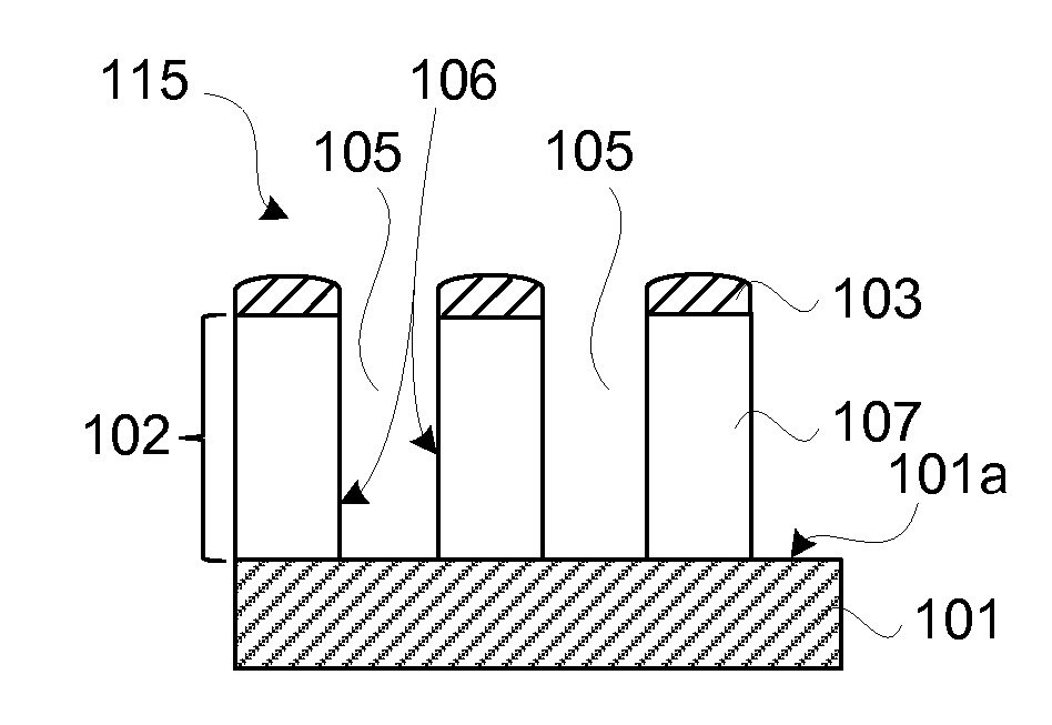
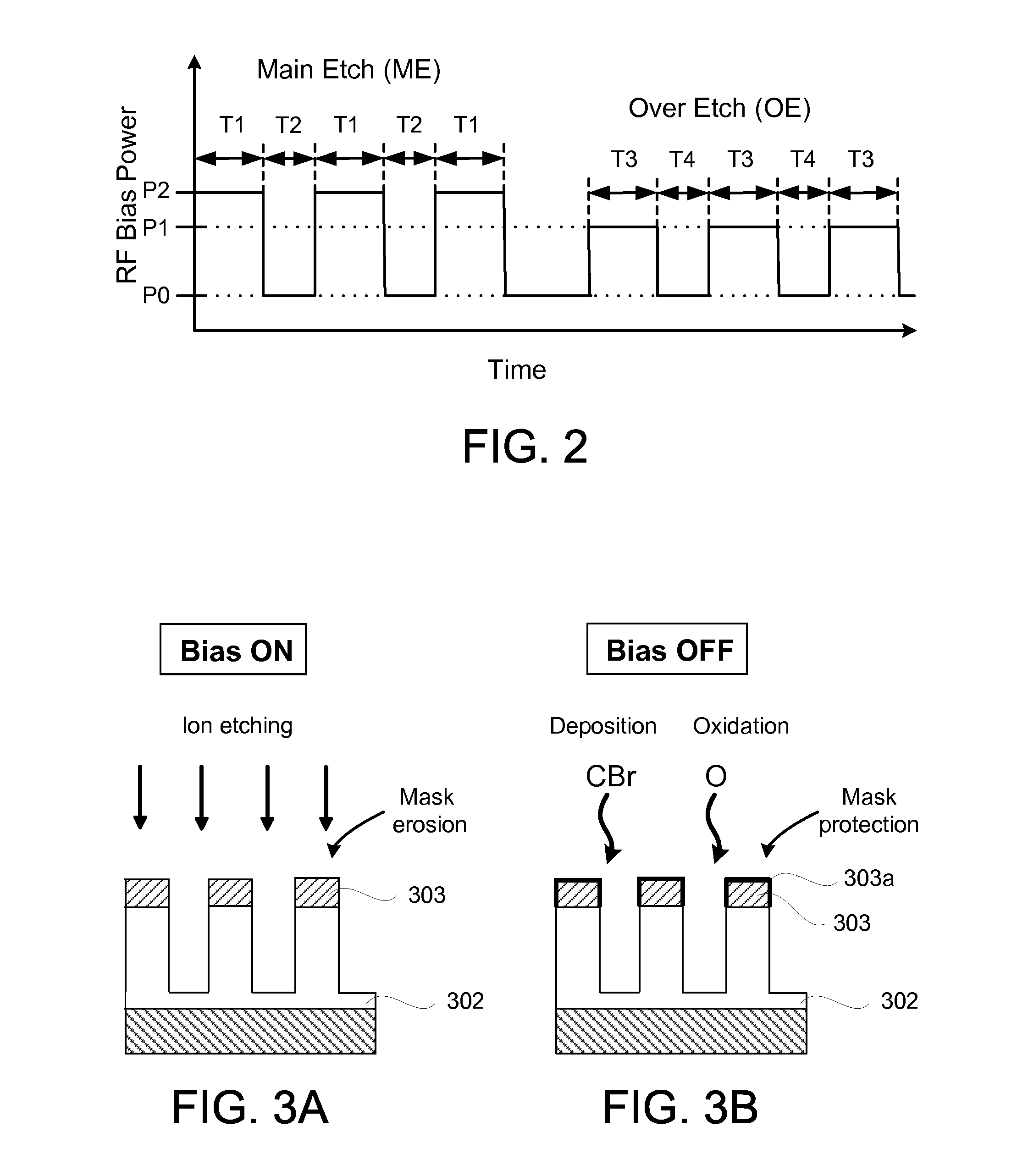
[0020]Embodiments of the invention are directed to a SiN plasma etching process that provides SiN etch features (e.g., trenches) with straight sidewall profiles and high etch selectivity of SiN to an overlying mask pattern and to a material at the bottom of the SiN etch features. In some embodiments, the SiN etch features are formed using a mask pattern cont...


PUM

PropertyMeasurementUnit
pressureaaaaaaaaaa
pressureaaaaaaaaaa
pressureaaaaaaaaaa

Abstract

A processing method is provided for plasma etching features in a silicon nitride (SiN) film covered by a mask pattern. The method includes providing a film stack on a substrate, the film stack containing a SiN film on the substrate and a mask pattern on the SiN film, transferring the mask pattern to the SiN film by exposing the film stack to a first plasma containing a carbon-fluorine-containing gas, O2 gas, and optionally HBr gas, and exposing the film stack to a second plasma containing a carbon-fluorine-containing gas, O2 gas, a silicon-fluorine-containing gas, and optionally HBr gas.

Description

[0001]The present application claims priority to U.S. provisional application Ser. No. 61 / 449,560, filed on Mar. 4, 2011, the entire contents of which are herein incorporated by reference.FIELD OF THE INVENTION[0002]1. Field of the Invention[0003]The present invention relates to a method for fabricating a semiconductor device, and more particularly, to a plasma etching method of silicon nitride (SiN) films using a patterned mask.[0004]2. Background of the Invention[0005]Many semiconductor fabrication methods employ plasma to perform etching processes where material on a wafer is removed in specific areas to subsequently form the components / features of the devices (e.g., transistors, capacitors, conductive lines, vias, and the like) on the wafer. The fabrication methods use a mask pattern that is formed over areas of the wafer that are to be protected from the etching process.[0006]During etching of deep features requiring long plasma exposure times, the mask pattern may be completel...

Claims


Application Information

Patent Timeline
Patent Type & Authority Applications(United States)
IPC IPC(8): H01L21/3065
CPCH01L21/3065H01L21/31116H01L21/31144
Inventor NISHIZUKA, TETSUYA
Owner TOKYO ELECTRON LTD
Features
  • Generate Ideas
  • Intellectual Property
  • Life Sciences
  • Materials
  • Tech Scout
  • Unparalleled Data Quality
  • Higher Quality Content
  • 60% Fewer Hallucinations
Learn More